About this article
This article provides you with important information about how we interpret and process your project data for the Amazing Assembly of your PCB.
Please read it carefully before submitting your assembly order and check if your design goes in line with the rules stated below.
TL;DR
We create an IPC-D-356A netlist when you upload a design using a supported format, the padnames and designators from the netlist are used to determine the component orientation and polarity. For components with 3 or more pads, the orientation is determined by the location of “Pad 1”, the orientation and polarity for components with two pads is determined by the IPC-7351B rules. (Except for Target3001!) . The component designator has to match our predetermined list. Only diodes, capacitors, inductors, and LEDs are specified in the IPC-7351 standard special cases are not automatically recognized.
Background
In theory, the silkscreen provides the assembler with all necessary information to identify the position and orientation of each component. However, the reality is different: Due to missing standardization and the immense variety of CAD applications, component types, and footprints, the silkscreen is not a secure source of information. And a few PCBs do not use silkscreen markings at all.
A better (yet not perfect) way to get more robust information about the component’s orientation is to evaluate the uploaded project file, as most of the applications respect the IPC rules for pad names in their standard footprints.
Component Orientation
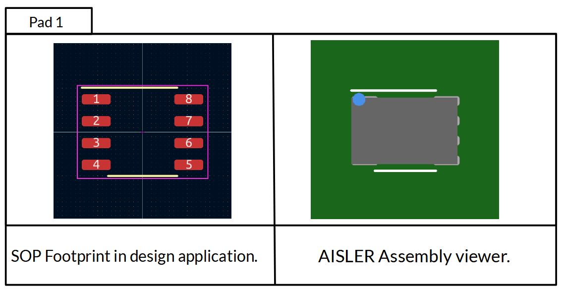
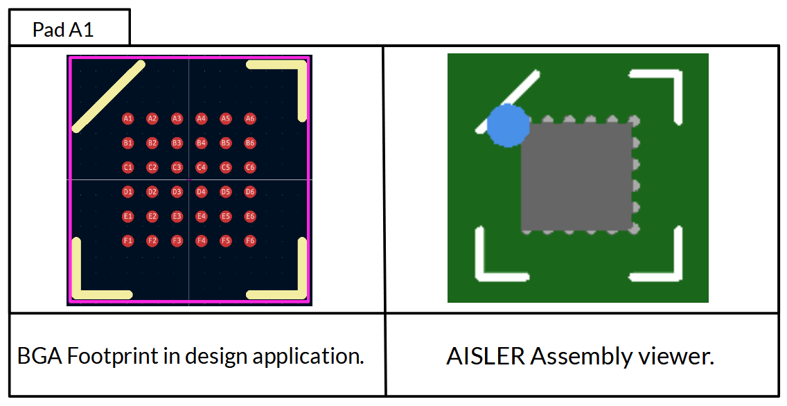
The orientation of components with 3 or more pads is determined by the location of the first pad, disregarding of the parts designators. We recognize pads with the names 1 and A1.
Component Polarity
The orientation and polarity of components with 2 pads is determined by the component’s designator prefix and pad names. We currently detect the polarity of capacitors (designator prefix C) and diodes (designator prefix D), the pad names need to obey the IPC-7351B rules with the exception of Target3001! designs, for more detail, please refer to the table below.

| Component | Capacitors | C | Diodes | E |
|---|---|---|---|---|
| Reference | “C#” (i.e. C5) | “D#” (i.e. D10) | ||
| Positive pole (+) | Negative pole (−) | Anode (+) | Cathode (−) | |
| KiCad | 1 | 2 | A, 2 | C, 1 |
| Altium | + | −, 2 | A | C, 1 |
| EAGLE, Fusion | + | −, 2 | A | C, 1 |
| Target3001! | 1 | 2 | 1 | 2 |
Limitations
We are aware of the limitations of the current implementation, and are actively working on a more accurate and flexible solution. At this time, we cannot account for special cases out of the box. Please contact our support if you require help.
Inspecting your design
We mark the first pin of components, cathode of diodes, and negative pin of polarized capacitors in our assembly viewer.
Please control each component and the assigned orientation and polarity! By submitting your order, you confirm the correctness of the assigned orientations.
Read more about how to use our assembly viewer and our rendering guarantee here: Rendering Guarantee for Amazing Assembly