Overview
In this article, we document our technical capabilities, how to interpret the board viewer and how-to design for manufacturability.
Technical Capabilities
| Min. Width | Max. Width | |
|---|---|---|
| Plated Slots | 0.7mm | 2.7mm |
| Non-Plated Slots | 0.8mm | No limit |
Milling
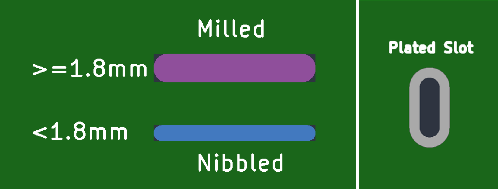
Non-Plated Slots with a width of 1.8mm or larger will be milled using the 1.8 mm or 2.4 mm milling tools. This is the preferred method to create slots.
Nibbling
Non-Plated Slots with a width less than 1.8mm and all Plated Slots will be manufactured using an industry standard nibbling process. Using this process, slots will be created by drilling several adjacent holes.

This offers the advantage that the amount of tool changes can be minimized at the expense of higher tool wear. As a result, the usage of smaller slots should be limited to applications where they are required. (USB-C connectors, DC-Jacks, Thermal cutouts for small sensors etc.) .
The slots width is automatically adjusted to account for the nibbling process, no changes on your side are required.
Please note: We employ a fair use policy for nibbled slots, and guarantee at least 75mm total length per PCB, if you use more, please contact our support.
Technical Limitations
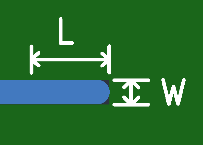
Minimal Length
The minimal length of a slot is limited to 1.5 times the diameter, as the nibble drill tends to skew when drilling very short distances. L > 1.5 x W
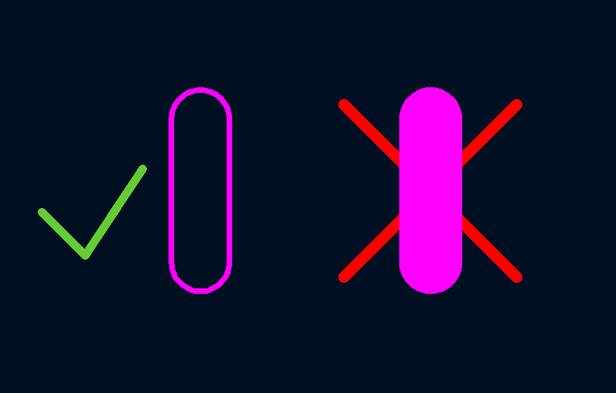
90° Corners
As nibble/milling bits are round, it is not possible to manufacture 90° corners.
The milling path supported by our tooling will be displayed in the board viewer.

EDA Design Guidelines
For the successful processing of your design, you need to follow our EDA Guidelines.
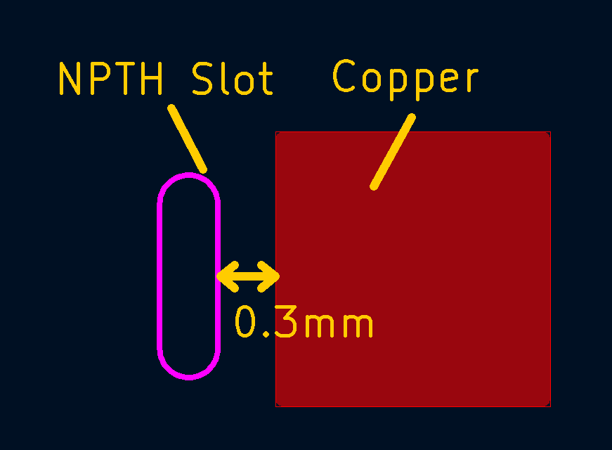
Non-Plated Slots
Non Plated slots need to be drawn on the board outline layer, do not use a filled shape.
Keep a distance of at least 0.3mm between a NPTH slot and any copper features.
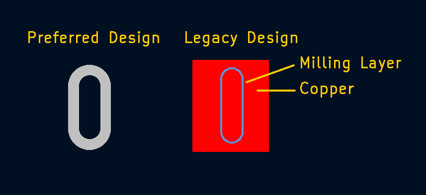
Plated Slots
Most modern EDA tools support plated slots, this is the preferred way of using them in your project.
Older legacy tools (like EAGLE) do not have this functionality, designers using such tools have to create a plated slot by drawing the slot using the milling layer inside a copper fill. Design examples for eagle can be found here: Plated Slots in EAGLE
Boardviewer
We give a guarantee on our renderings, you should always use the Board Viewer to check if the slots are properly processed.
Plated & Non-Plated Slots
- Plated Slots will not be marked, which means you can see the black background of the viewer.
- Non-Plated Slots above 1.8 mm width will be milled and marked in a purple color.
- Non-Plated Slots under 1.8 mm width are nibbled and marked in a light blue color.
Processing Notes
The processing notes in our Board viewer inform you in case your slots cannot be manufactured the way they were specified, or your design is problematic in other ways.
Critical use of elongated holes
This note informs you that the length of slots which will be nibbled exceeds our fair use policy, you will not be able to order the design without further approval from our engineers. Please contact our support.
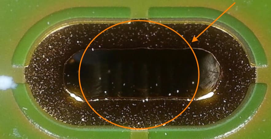
Inner milling paths missing and/or Incomplete
This note informs you that the slots cannot be manufactured the way you specified it in your design. You can click on the processing note to highlight the problematic area in yellow.
In this example, we would not be able to manufacture the entire slot within the specified radius, only the blue highlighted areas would be nibbled.

These slots would not be manufactured because the width specified in the design is smaller than what is supported with our tooling.