UAH Motorsport – BMS Cell Sensing & Fuse PCB
Shareable project link:
Hi AISLER Community,
We are UAH Motorsport, a multidisciplinary Formula Student team formed by students from different engineering and university degrees at the University of Alcalá (Universidad de Alcalá), Madrid, Spain.
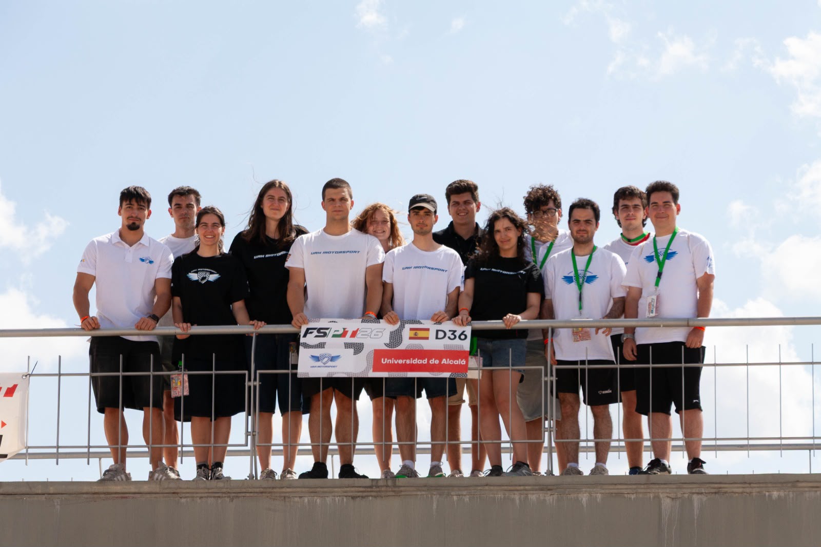
Our team designs and develops a Formula Student single-seater from the ground up, bringing together mechanical, electrical, electronic and software engineering. The project gives students the opportunity to apply university knowledge to a real motorsport engineering environment, where every subsystem has to be designed, manufactured, integrated and validated as part of a complete vehicle.
During the 2026 season, we participated in Formula Student Portugal in Class 2, where we achieved 2nd place in Engineering Design. As this was one of the first stages of development of our electric vehicle, much of the season was focused on the design, engineering justification and validation of the different vehicle systems.
We are now moving from that design phase into manufacturing, testing and vehicle integration, turning the systems developed during the previous season into real hardware.
One of the most important areas of this development is the high-voltage accumulator and its Battery Management System (BMS). For this reason, we are developing several custom PCBs dedicated to cell monitoring, temperature acquisition, communication, protection and integration of the accumulator electronics.
This Cell Sensing & Fuse PCB is one of those boards.
It is designed to provide a compact and organized interface between the accumulator cell voltage taps and the main BMS electronics, while integrating the fuse protection required for the individual sensing lines.
This board will also be one of the first PCBs manufactured as part of our collaboration with AISLER, whose support is helping us move our electronics from design and validation into real manufactured hardware.
1. Why did we start this project?
Our high-voltage accumulator is divided into several removable battery segments. Each segment contains multiple series-connected cell groups whose voltages must be individually monitored by the BMS.
This means that a significant number of cell-sensing connections have to be routed from the accumulator cells to the BMS measurement electronics.
Instead of managing all of these connections only through the wiring harness, we decided to develop a dedicated Cell Sensing & Fuse PCB.
The main objectives of the board are to:
- provide an organized interface for the individual cell-voltage sensing connections;
- integrate the fuse protection associated with these sensing lines;
- simplify the accumulator wiring architecture;
- improve repeatability during assembly;
- facilitate inspection and troubleshooting;
- reduce the complexity of the internal sensing harness;
- provide a more controlled connection between the accumulator cells and the BMS electronics.
The board forms part of our modular BMS architecture based around the Analog Devices ADBMS6830 multicell battery monitoring system.
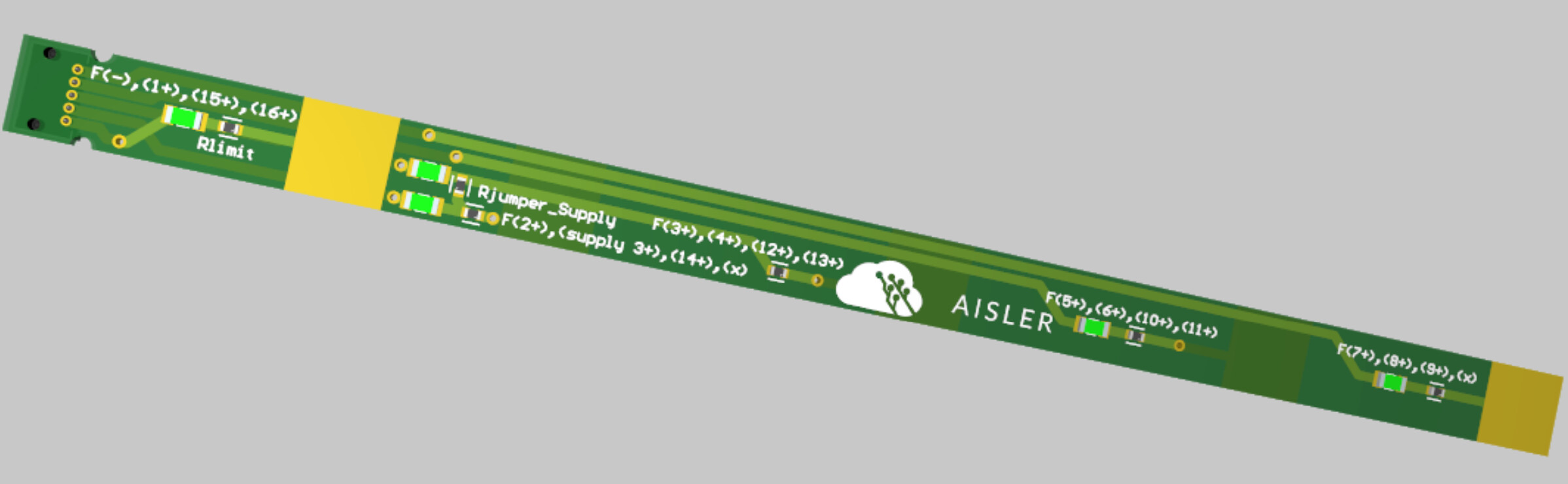
One of the most characteristic aspects of the design is its geometry. The PCB is extremely long and narrow because it has been designed around the available mechanical space inside the accumulator segment.
In this case, the mechanical architecture of the battery strongly influenced the electrical design of the PCB.
2. What do we love about electronics?
One of the aspects we find most interesting about electronics in Formula Student is that a PCB is never only an electrical circuit.
The final design has to simultaneously consider:
- electrical performance;
- mechanical integration;
- connector accessibility;
- manufacturing constraints;
- reliability;
- serviceability;
- safety;
- assembly procedures;
- interaction with the wiring harness and the rest of the vehicle.
This PCB is a good example.
From a purely schematic perspective, its function is relatively straightforward: route the individual cell sensing connections and integrate their associated protection components.
However, transforming that electrical function into a board that can actually be installed inside a compact Formula Student accumulator introduces a completely different set of engineering constraints.
The unusual geometry, component placement, connector location and routing of the sensing lines all have to be considered together.
This interaction between different engineering disciplines is one of the reasons why developing electronics for a Formula Student vehicle is particularly interesting for us.
3. Which PCB Design Tool do we use and why?
For our PCB development we use Altium Designer.
It allows us to manage the complete electronics development workflow within the same environment, including:
- schematic capture;
- component libraries;
- PCB layout;
- routing constraints;
- design rules;
- layer stack configuration;
- mechanical information;
- 3D visualization;
- manufacturing outputs.
For this particular PCB, the 3D environment has been especially useful.
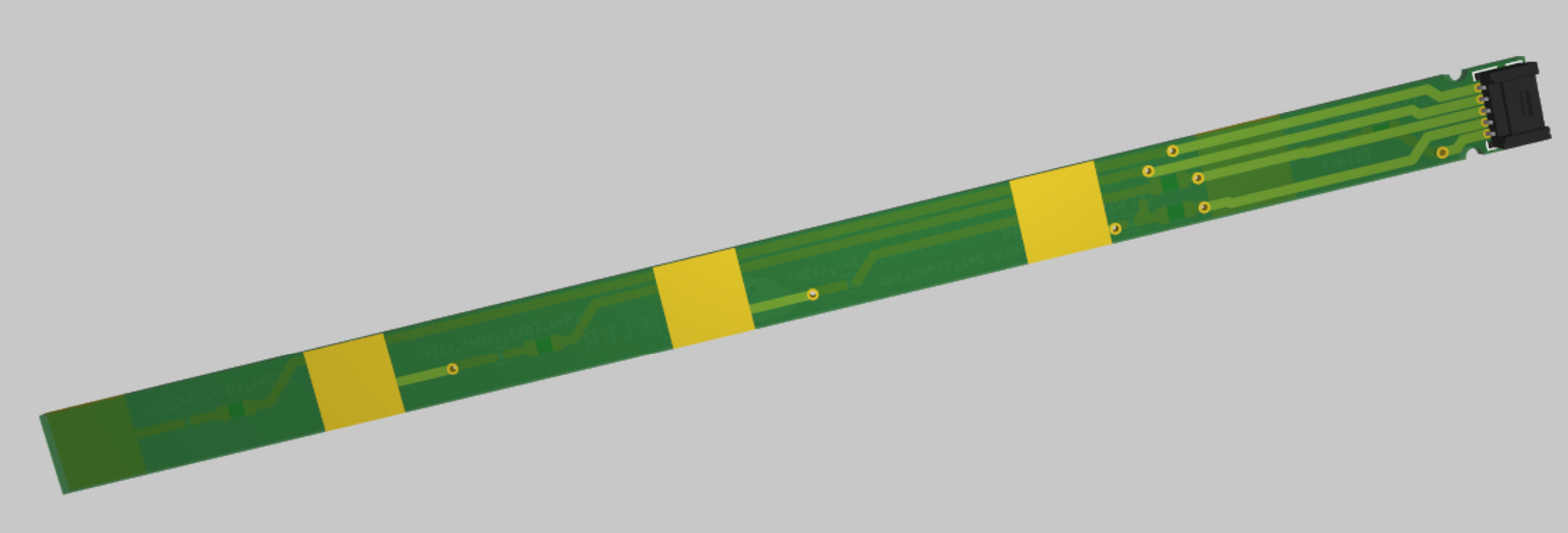
Because the board has a very high length-to-width ratio and has to fit within a restricted area of the accumulator segment, mechanical verification is an important part of the design process.
Using the 3D model allows us to check the relative position of the PCB, connector, components and mounting regions before manufacturing the board.
It also helps us detect mechanical integration issues earlier in the design process instead of discovering them after fabrication.
4. What was our greatest challenge with the project?
The main challenge of this PCB has been the combination of mechanical packaging and electrical routing.
The available space inside the accumulator results in a very long and narrow PCB. Consequently, the different cell-sensing signals have to travel along a relatively constrained routing area.
Unlike a more conventional rectangular PCB, there is very little freedom to redistribute components or signals across the board.
The design therefore required several iterations to optimize the relationship between:
- PCB outline;
- component positioning;
- connector location;
- sensing-line routing;
- fuse placement;
- mechanical clearances;
- available copper area;
- integration with the accumulator structure.
Another important consideration was maintaining a design that remains understandable and serviceable.
In a competition vehicle, the PCB does not only have to work electrically. It must also be possible to inspect it, identify individual cell connections and diagnose a potential fault during testing or maintenance.
For us, this has been one of the most valuable parts of the project: understanding how strongly the mechanical design of the accumulator can influence what initially appears to be a relatively simple electronic board.
5. What is our greatest win in the project?
One of the main achievements of the project is converting part of the cell-sensing architecture from a potentially complex collection of individual wiring connections into a dedicated and structured PCB interface.
This gives us a much more controlled way of connecting the accumulator cell groups to the BMS.
From an engineering perspective, the board improves several aspects of the system:
- the sensing architecture becomes easier to document;
- cell connections are easier to identify;
- assembly becomes more repeatable;
- integration with the wiring harness is simplified;
- the fuse protection is incorporated directly into the sensing interface;
- the resulting system is easier to inspect and maintain.
Another important milestone has been reaching a PCB geometry that can perform its electrical function while adapting to the restricted mechanical envelope available inside the battery segment.
Seeing the complete design assembled in the 3D environment after several iterations is an important step before moving into manufacturing.
The next objective is now to manufacture the boards and begin physical validation.
6. What is our favorite AISLER feature?
One of the features we particularly appreciate about AISLER is that the platform is not limited to PCB manufacturing.
The combination of the manufacturing service with the technical documentation and the AISLER Community provides useful information during the design stage itself.
Being able to consult manufacturing capabilities, PCB specifications and design recommendations while developing the board helps us consider manufacturability before the design is finished.
For a Formula Student team this is especially useful, because our PCBs are developed by students and the manufacturing process is also an important part of the learning experience.
We have also integrated the AISLER logo directly into the PCB silkscreen, as can be seen in the 3D render of the board.
This PCB represents one of the first manufacturing steps of our collaboration with AISLER, and we are looking forward to receiving the physical boards, assembling them and validating their operation inside the accumulator.
Once the PCBs arrive, our next stages will include electrical verification, continuity testing, integration with the BMS electronics and validation of the complete cell-sensing system.
We are also looking forward to sharing future developments, manufacturing progress and the final integration of these electronics into our Formula Student car with the AISLER Community.
Many thanks to AISLER for supporting UAH Motorsport and student engineering.