Hello, we are currently designing a couple of boards using a 0.5mm pitch BGA with a rather friendly landing pattern. It is a NXP MCXA144VMP with 64 pins on a 9x9 grid.
The problem: Aisler’s minimum via size is just a tiny bit too large.
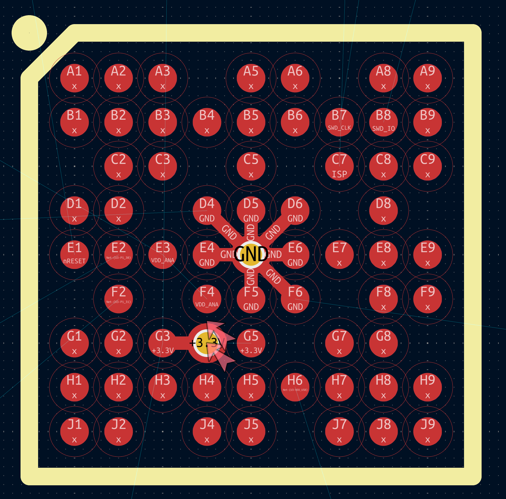
As you can see in the screenshot, the 3.3V has two types of violations:
Net Clearance Violation (0.125mm, actual 0.114mm) and Hole Clearance Violation (0.25mm, actual 0.214mm)
Fan out is not a problem because I only ever need two of the three signals from the inner row (fortunately).
Now I wonder what my options are. Changing the package is unfortunately not possible.
Are these violations a big deal, or are they insignificant enough that I could ignore them?
Two ideas came to mind:
-
How about if I cut away a tiny segment from the via annular ring where needed? This could deal with the net clearance violation while still leaving the annular ring mostly intact. It won’t help with the hole clearance though.
-
What about the idea of changing the affected pads of the BGA slightly? I was thinking of a symmetrical superellipse with the same area as the circular pad. (Kind of a morph between a rounded rectangle and a circle).
That could solve both issues. I guess the auto-centering of the BGA pads won’t be affected because the superellipse would be symmetrical and quite circular. But I have never done this, so I thought I’d better ask.

I wonder what tweaks you would recommend for me. I’m certainly not the first one to run into this problem, and Aisler knows its process best, so some recommendations would be greatly appreciated.