Hello!
For PCB trace impedance calculation, I am using and recommend Saturn PCB Design Toolkit. It is a small and free Windows program that has numerous useful calculators, including RF line calculator.
In Saturn PCB Design Toolkit, there are 4 parameters that participate in calculation: Trace width, Trace-to-trace clearance, PCB thickness, and PCB dielectric constant.
For simple projects, I always use 0.2mm trace-to-trace clearance, because ir is very robust, any PCB manufacturer can produce such PCBs at lowest price. Going under 0.2mm becomes hard, as it may increase cost and X-out on panels.
In Aisler, there are only 1.6mm thick PCBs, so that number is also fixed. And I actually recommend 1.6mm PCBs because thinner PCBs warp a lot more during reflow soldering, so unless it is totally necessarry, using 1.6mm gives flat, strong and robust PCB.
For dielectric constant, that one is the most problematic, but I usually use FR-4 STD, which defaults to 4.6.
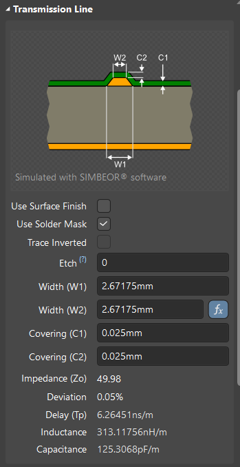
The final parameter is trace width. This one you just have to type in different values, until impedance is close enough to what you need. I personally use 1.25mm width, which gives 49.5767 Ohms. And yes, it is VERY thick trace, that is true.
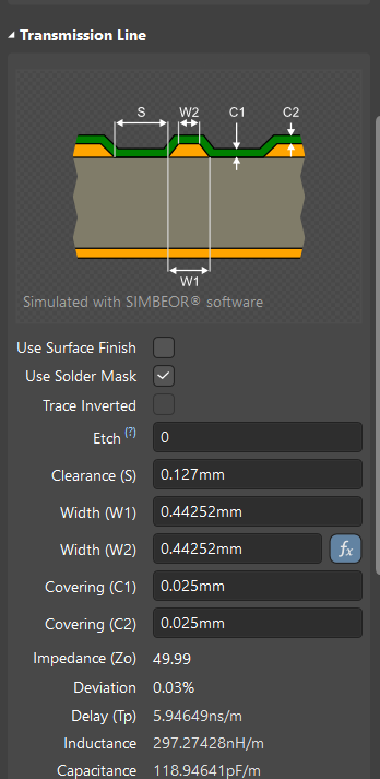
If you were to use 0.1mm gap between trace and ground plane, you could have 0.7mm wide trace.
However, note that Saturn calculations differ from Altium calculations  Probably because in Altium, you can specify more info about your PCB - thickness of each layer (copper, prepreg, dielectric, soldermask, silkscreen) and also their dielectric constants. So maybe that is why it gives a bit different result. Because underlying physics and formulas are the same, just more info goes into Altium. My computer and wallet cannot run latest Altium Designer, so I use Altium CircuitStudio and Saturn PCB Toolkit.
When using 4-layer PCB, the gap between Top layer and Internal Layer 1 is only about 0.1mm, so trace width can also go down: with Er=4.6, trace width 0.2mm and trace-to-trace clearance 0.2mm, the impedance is 51.62Ohms. And don’t worry about not getting precisely 50.000 ohms! Because, to create PCBs with REAL impedance control, one has to pay more attention to etching precision, not so much on trace width.
Also, impact of each parameter can be found in this excellent Wurth Elektronik applicatin note:
Best regards,
Andris Igaunis