4-Layer HD PCB Stackup

Stackup for 4-Layer Boards

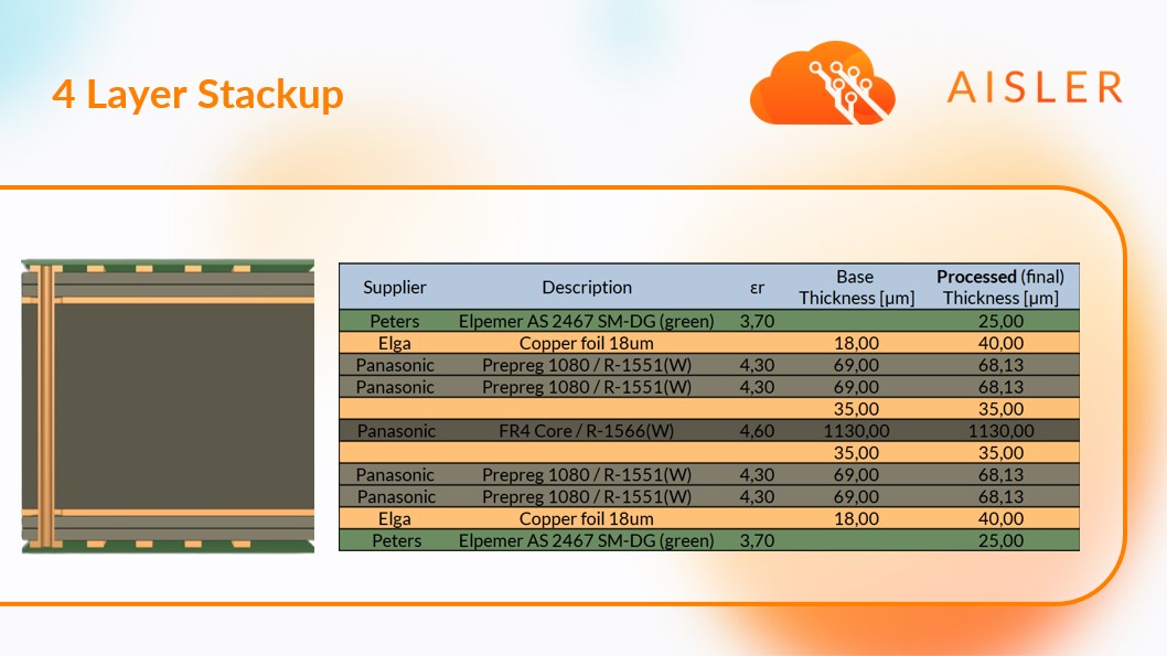
We use Panasonic Prepreg 1080 Type R-1551(W) (58.9 KB), Peters coatings and Elga Copper foil.

Our Boards are RoHS and REACH compliant.

The following track layouts can be used to realise defined impedances. Please note that these values only provide a basic orientation. Interference factors such as angles, meanders or vias in the routing of the tracks may have a negative effect on the intended impedances.

Type Impedance Signal- / Reference Layer width space width
Single Ended 50 Ω TOP / IN1, BOT / IN2 245 µm - -
Differential pairs 90 Ω TOP / IN1, BOT / IN2 230 µm 165 µm 230 µm
Differential pairs 100 Ω TOP / IN1, BOT / IN2 190 µm 180 µm 190 µm
2 Likes

Looking at the 4L HD stack-up picture above I’m confused/concerned (accurate loss and trace-trace coupling calculations) about the true thickness of the outer copper layers. It says 18um copper foil, but a processed thickness of 40um. How does 18um become 40um? Surely your ENIG coating isn’t 22um thick.
Speaking of ENIG, Nickel is magnetic and causes considerable loss in high-speed/high-frequency signals. Is there a way to order WITHOUT ENIG coating?

1 Like

Hello @justatoms,

welcome to the community!

The final copper thickness of 40 µm is the result of the 18 µm base copper of the copper foil plus approx. 22 µm copper, which is applied by the electroplating process.

2 Likes

Thank you Manuel,

Pardon my ignorance on PCB manufacturing.
Am I correct then in assuming this 22um Cu plating being the result of the same (electroless) plating process that creates the PTH vias?

Will copper under the soldermask be ENIG plated?

Thanks,
Anne

1 Like

Hello Anne,

correct, this electroplating process is the key process step that leads to the formation of a conductive copper sleeve in the borehole of each PTH.

The ENIG coating is applied after the soldermask has been applied. Consequently, the copper structures below the soldermask are not coated.

Best regards,
Manuel

2 Likes

Hello Aisler Team,

I have a question about your Soldermask: Why is it getting lighter on the outside? Is it getting thinner there due to surface tension?

The picture was taken from Plated and Non-Plated Slots and Cutouts, I have seen it on my boards I odered from you too in the past.

Thank you. :cowboy_hat_face:

Hello Aisler team,
do you have recommended W and W/S for the most popular transmission lines impedance, such as SE45, SE50, Diff85, Diff90, Diff100, possibly based on past experiences with this stackup or, even better, real world measurements?
Those numbers would be very helpful.

Many thanks!

Best regards,
Giacomo

Hello Andreas,

I am sorry for the late reply.

Correct, this effect is due to differences in the thickness of the solder resist. The electroplating process builds up tracks and surfaces with additional copper. However, this build-up does not occur completely evenly across the entire width of the track/surface. Thus, any copper structure has more a trapezoidal or dyke-like shape in cross-section rather than a rectangular shape. On the slopes, the solder resist has less adhesion and therefore forms thinner.

Best regards,
Manuel

1 Like

Hi Giacomo,

welcome to the community and thank you for your request!

I will try to make this information available here as soon as possible.

Best regards,
Manuel

Track layouts for SE50, Diff90 and Diff100 are now listed below the stackup information!

1 Like

Is this now the actual 4 layer stackup or are there any changes that aren’t updated in the image above?

Hi @Jan_Richert-web-de ,

Welcome to the community!

Yes, the stackup is up to date!

Best regards,
Manuel

Hallo!
I’m looking into making a 4 layers board, and I have questions regarding vias. Is it possible to make a via that links only two contiguous layers (for example, on KiCad, F.Cu and In1.Cu)?

Self replying to mention I found the proper terminology: I’m talking about blind vias.

Aisler does not support blind vias at the moment.

Hi there for the defined impedance table, could you also list the type of transmission line?
Like, is it a micro-strip, or a coplanar wave-guide with ground for example? :slight_smile:

The impedance calculations refer to microstrip and coupled microstrip lines.