Hi,
any chance to get an alternative 4 layer stackup? The 245 µm trace width for 50 Ohm is a little limiting. With e.g. a 0.12 mm prepreg it could be reduced to ~185 µm…
Cheers,
Johann
Hi,
any chance to get an alternative 4 layer stackup? The 245 µm trace width for 50 Ohm is a little limiting. With e.g. a 0.12 mm prepreg it could be reduced to ~185 µm…
Cheers,
Johann
You can contact our support regarding alternative stackups for volume production.
We only offer the current stackup, this way we are able to offer better prices and turnaround time for everyone. Would your design allow for a grounded coplanar waveguide? This could help getting the tracewidth smaller.
Thanks for the fast response!
I want to route out the gpios of an raspberry pi compute module 4 with 50 Ohm. With the cm4 connector having a two row 0.4 mm pitch, this is basically impossible with 245 μm tracks. And the 138 μm prepreg also suggests a quite large 280 μm track clearance…
I do understand that offering only 1 stackup is most cost effective. Do you maybe have any plans to change the existing one? Or am I the only one asking??
I‘m just an hobbyist, so no mass production planned… ![]()
We currently do not plan to change it.
May I ask why you want to use 50 Ohm traces for the GPIOs? The CMOS output stages are to my knowledge not impedance matched. The idea of controlled imedance is to reduce signal reflection 50Ohm was just chosen as a value that is easily manufacturable. Something slightly lower or higher will not be an issue for just GPIOs. Other factors like good decoupling or return paths are more important. The thight pinout of the CM4 connector is quite the edgecase.
50 Ohms is not an absolute must, basically something which I use by default as it‘s “never wrong“. The necessary clearance of 2H for appropriate crosstalk reduction bothers me more. I have too many parts (DSI connector, CSI connector, RTC, Fan controller, USB hub and more) to place, so that I cannot afford the track clearance, even when routing on top and bottom. Also the 90 and 100 Ohm differential pairs (which are mandatory) seem difficult for what I want to pack onto a 10x10 cm board. Your process seems to allow 125 µm width and clearance, but the prepreg thickness doesn‘t seem to allow me to use it for this particular project.
I‘m still glad that I was pointed to aisler. Your support (responses this fast late evening, wow!) is convincing and I like the no frills approach. For further projects I‘m sure I will check again!
I am aware of the shortcomings when it comes to high density designs with our stackup.
Would using 6 Layers be an option to you? This could give you more room for the traces.
I appreciate your feedback and I will bring it up when we decide to expand our portfolio.
6 layers are an interesting idea. I thought a little about it, but I guess it will not work out for me:
Additionally I identified other constraints in your HD boards which will not work for me:
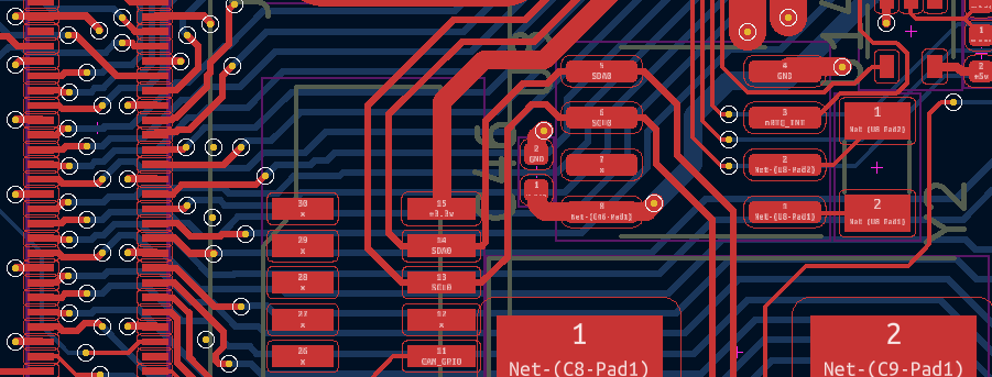
I’m attaching a screen shot of how I’ve done the boards. Vias are 0.5 and traces are 0.185 with a clearance of 0.240. I guess you are simply not targeting this kind of boards at the moment. Maybe in the future… ![]()