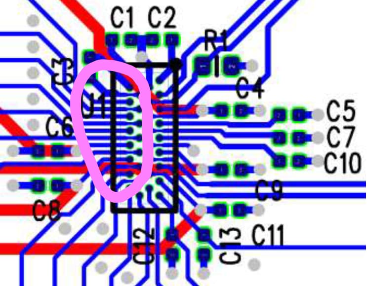
We are currently investigating using Aisler for more of our production of our prototypes but seem to be coming up against some limitations in the capabilities. We use a DA7212 codec on several of our designs which, according to the datasheet can be “routed
using conventional, low cost, PCB technology, all device balls are routable on the top level”. With our current prototype supplier we actually use micro-vias for the middle rows of pads but we know that Aisler don’t offer micro-vias. Is there any way we could produce a design with this chip with Aisler?
For little more info, the chip has a pitch in the vertical direction of 0.5mm with a ball width of 250um. Using IPC calculator to calculate the pad size as 200um, which seems to be within the capabilities of Aisler. However, this only leaves 300um to route the trace out. Could we risk necking-down to 100um track width with 100um clearance either side? Or would we have a better chance with reducing the pad size to 150um or even 125um for best results? Or would this be dumb to try and have no chance of working? Any input would be warmly welcomed ![]()
If we did decide to “chance it” and go ahead with production (I understand there would not be a 100% yield), could you test with flying leads or optical inspection all traces from this BGA package for continuity and shorts?
