Hello Aisler Community,
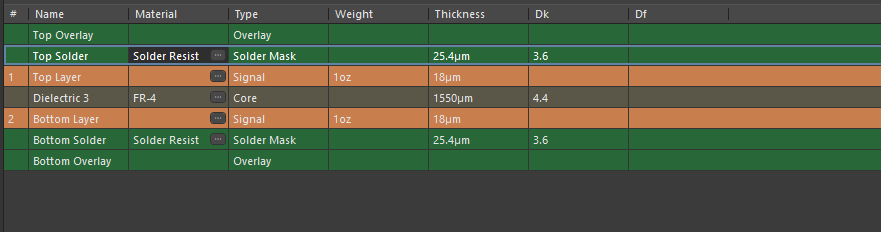
I am currently in the process of designing a 2-layer PCB and have come across some confusion regarding the correct way to configure the stackup based on the information provided on the Aisler website. It’s not entirely clear to me whether I should be using the “Process Thickness” or the “Base Thickness” for my design. Additionally, I’m unsure if my current stackup configuration is correct and would greatly benefit from some guidance on this.
Could someone please provide more detailed information or clarification on how to accurately configure a 2-layer PCB stackup? Moreover, an article or resource with more comprehensive details on stackups for 2-layer and 4-layer PCBs, possibly with examples for popular design tools like Altium, Fusion, and Eagle, would be incredibly helpful. Such resources would greatly aid in ensuring that designs meet the required specifications and quality standards.
Thank you in advance for your assistance and support. The Aisler Community’s expertise is invaluable, and any insights or resources you could share on this matter would be deeply appreciated.
Best regards,