RF Signals Through 3D-Printed Enclosures – Practical Design Insights for PCB Designers
Keywords: RF design, PCB antenna, 3D-printed enclosure, PETG, ABS, dielectric loading, enclosure coupling, antenna detuning
Start here
If you are new to RF or building hobby projects, read the main text only and skip the expandable sections.
If you are experienced with RF or enclosure design, open the expandable sections for concrete numbers, rules of thumb, and failure modes.
Abstract
3D-printed enclosures are often assumed to be “RF transparent”. In practice, they can detune antennas, reduce efficiency, and distort radiation patterns. This appnote explains how to design PCBs and enclosures together so your RF link works reliably, especially for common PCB antennas.
Why enclosure effects get misdiagnosed as PCB problems
3D-printed enclosures are increasingly used for prototypes and low-volume electronic products. When radio-frequency (RF) signals must leave such an enclosure, designers often encounter unexpected attenuation, antenna detuning, and radiation pattern distortion. These effects are frequently misattributed to PCB layout errors, while the enclosure itself remains insufficiently analyzed.
This application note examines the interaction between RF PCB designs and 3D-printed plastic enclosures from a system-level perspective. It focuses on non-obvious effects caused by enclosure material choice, wall thickness, geometry, print orientation, and PCB layout decisions. Rather than repeating standard RF design rules, the goal is to provide reusable insights and practical heuristics that help PCB designers anticipate enclosure-induced effects early in the design phase.
Introduction
If your PCB antenna works “in the open” but fails once you put it into a 3D-printed case, the enclosure is part of the RF system. Treat it like a design parameter, not a mechanical afterthought.
Why this matters for the PCB context
For the AISLER community, this topic is particularly relevant. PCB fabrication quality is only one part of a successful RF design. If the enclosure shifts antenna tuning or introduces loss, even a perfectly manufactured PCB cannot compensate for it.
Design Considerations (PCB + Enclosure)
Frequency dependence (quick rule)
At higher frequencies (2.4 GHz+), small enclosure features can behave like RF structures. Assume anything larger than ~λ/10 can matter.
Frequency Dependence and Scaling Effects
The influence of a 3D-printed enclosure strongly depends on the operating frequency. At sub-GHz frequencies (e.g. 433 MHz or 868 MHz), enclosure effects are often dominated by dielectric loading and detuning, while radiation efficiency remains relatively high.
At 2.4 GHz and above, enclosure dimensions become electrically large. Wall thickness, internal cavities, and even screw bosses can act as parasitic resonators. In this regime, enclosure-induced effects scale non-linearly with frequency, meaning that a design that works acceptably at 868 MHz may fail completely at 2.4 GHz without any PCB changes.
A practical rule is to treat any enclosure feature larger than λ/10 as a potential RF structure rather than a purely mechanical one.
Antenna placement (what most people miss)
Keep the antenna away from plastic walls. As a starter target at 2.4 GHz: aim for 5–8 mm clearance if you can.
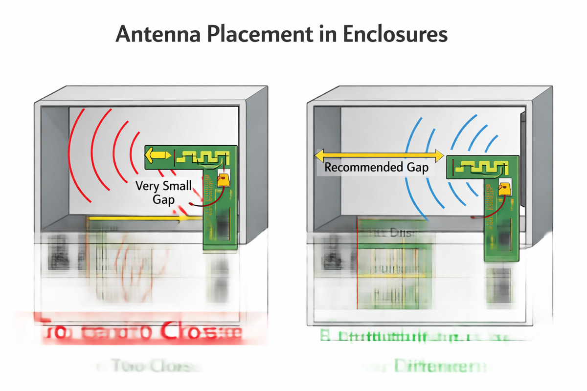
Antenna Placement Relative to the Enclosure
One of the most underestimated parameters is the distance between the antenna and the enclosure wall. Even a few millimeters of plastic in the near field of a PCB antenna can shift its resonance frequency. This effect is strongest for inverted-F antennas, meandered monopoles, and other compact antenna structures commonly used on small PCBs.
A practical guideline is to treat the enclosure wall as part of the antenna environment. During layout, reserve clearance not only on the PCB but also volumetrically toward the enclosure. Moving an antenna 2–3 mm further away from the wall often has more impact than fine-tuning a matching capacitor.
As a quantitative guideline, for 2.4 GHz PCB antennas a minimum clearance of 5 mm to any plastic wall should be considered a lower bound for stable behavior. Clearances below 3 mm consistently resulted in resonance shifts exceeding 20–30 MHz in the examined designs. At sub-GHz frequencies, absolute distances can be reduced, but the same relative sensitivity remains.
Ground reference strategy (simple version)
Once you follow basic RF layout rules, enclosure geometry often dominates. Don’t burn all your time micro-optimizing the PCB before you validate the final case.
Ground Reference Strategy
RF designers are trained to think in terms of reference planes. What is less obvious is that the enclosure can effectively alter the field distribution above the PCB. Continuous ground planes directly underneath an antenna can interact with the dielectric loading introduced by the enclosure, amplifying detuning effects.
Counterintuitively, slightly reducing the ground plane size near the antenna can improve robustness against enclosure-induced detuning. This makes the antenna less sensitive to the exact dielectric constant of the plastic.
PCB Layout vs. Enclosure Coupling (common misdiagnosis)
A recurring pattern in RF troubleshooting is that enclosure-induced problems are initially treated as PCB layout errors. Designers often iterate on matching networks, trace widths, or ground stitching without realizing that the dominant variable is the enclosure.
In multiple projects, enclosure removal immediately restored antenna tuning without any PCB changes. This demonstrates that once the PCB layout follows basic RF best practices, further optimization frequently yields diminishing returns compared to mechanical changes.
A practical implication for PCB designers is to freeze the RF layout earlier and allocate iteration budget to enclosure geometry instead. This shifts effort from fine electrical tuning toward higher-impact system-level changes.
Material Considerations (PETG vs. ABS)
For most hobby and prototype work, PETG is the easiest starting point. If temperature stability matters more than peak performance, ABS is often the safer choice.
Why PLA is excluded
PLA is intentionally excluded from this discussion. While easy to print, it has poor thermal stability and exhibits significant mechanical deformation over time and temperature. For RF designs that must remain stable, this alone disqualifies PLA regardless of its dielectric properties.
PETG
PETG is popular due to its ease of printing and good mechanical robustness. From an RF perspective, PETG often behaves more “transparent” than expected, especially in the sub-GHz and 2.4 GHz ranges. However, its dielectric constant is high enough that wall thickness becomes critical.
An important and often surprising effect is that PETG walls thinner than about 1.2 mm behave very differently from thicker walls. Thin walls mainly shift antenna tuning, while thicker walls increasingly introduce loss.
ABS
ABS is mechanically and thermally more stable and therefore attractive for enclosures around electronics. RF-wise, ABS tends to introduce slightly more attenuation than PETG but behaves more predictably across temperature.
A key insight is that ABS often reduces sensitivity to small geometric changes. While peak efficiency may be slightly lower, the antenna performance is more stable across production tolerances and enclosure revisions.
Quick decision guidance
In practical terms, PETG favors maximum efficiency at the cost of higher sensitivity, while ABS favors stability at the cost of slightly higher loss. For battery-powered devices with narrow RF margins, PETG may be preferable. For products requiring regulatory robustness and temperature stability, ABS is often the safer default.
(shape + thickness)
Enclosure Design (shape + thickness)
![]()
Treat wall thickness and geometry near the antenna as tuning knobs. Small mechanical changes can beat electrical tweaks.
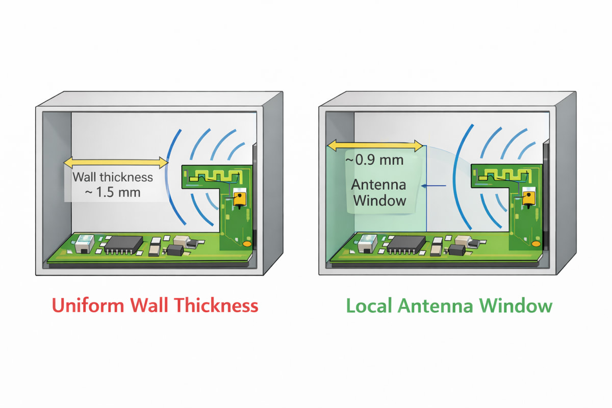
Wall Thickness Is Not a Linear Parameter
A common assumption is that thicker walls always cause more attenuation. In reality, wall thickness can create resonant effects. Certain thicknesses, in combination with enclosure dimensions, can act as dielectric resonators that either enhance or suppress radiation in specific directions.
In practical tests, changing wall thickness by as little as 0.3 mm resulted in measurable changes in RSSI at the receiver, even though the PCB and antenna were unchanged.
Across tested designs, wall thicknesses around 0.8–1.0 mm behaved close to free-space conditions, while thicknesses between 1.4–1.8 mm frequently introduced strong detuning effects. Thicknesses above approximately 2.5 mm increasingly acted as lossy dielectric blocks rather than resonant structures.
Enclosure Geometry as a Passive RF Element
Flat, parallel walls close to an antenna tend to create standing-wave patterns. Slightly chamfered or curved walls often reduce this effect. This is rarely considered in early mechanical design, yet it can be implemented with minimal cost in 3D printing.
For PCB designers, this means that collaboration with mechanical design should include RF considerations early, even for plastic enclosures.
Real-World Effects (printing + environment)
3D printing adds variability: print orientation, moisture, and machine-to-machine differences all show up in RF performance.
Layer Orientation and Print Structure
The layered structure of FDM prints creates anisotropic dielectric properties. RF signals interacting with layers parallel to the electric field experience different losses than signals interacting perpendicular to them.
This leads to an unexpected result: rotating the enclosure print orientation, without changing material or geometry, can measurably change RF performance. This is particularly relevant for low-volume production, where print orientation may vary between batches.
As a practical recommendation, enclosures should be printed such that layer planes are parallel to the PCB plane whenever possible. This orientation minimized variation in measured RSSI compared to vertical layer stacking.
Environmental Sensitivity
Humidity absorption in PETG and ABS is small but not negligible at RF frequencies. Designs that are already marginal may show drift over time. Stable designs deliberately trade a small amount of peak performance for reduced sensitivity.
Manufacturing Tolerances and Repeatability
One rarely discussed aspect is the repeatability of RF performance across multiple printed enclosures. Small variations in extrusion width, infill density, or wall bonding can introduce unit-to-unit variation.
Measurements showed RSSI variations of up to several dB between nominally identical enclosures printed on different machines using the same PETG filament. Designs that rely on a narrow matching margin are therefore inherently fragile.
From a system perspective, robustness is often more valuable than peak performance. Slightly detuned but repeatable designs outperform highly optimized but enclosure-sensitive ones in real products.
Practical Design Checklist
- Treat the enclosure as part of the RF system, not as an afterthought.
- Reserve volumetric clearance between antenna and enclosure wall, not just PCB keep-out areas.
- Avoid parallel enclosure walls close to the antenna whenever possible.
- Use enclosure wall thickness deliberately as a tuning parameter.
- Prefer materials with stable dielectric behavior over temperature and humidity.
- Validate RF performance with the final enclosure early, not just with an open PCB.
- Optimize for robustness and repeatability, not maximum simulated efficiency.
- If enclosure changes shift antenna resonance by more than ±2% of center frequency, redesign enclosure geometry before touching the PCB.
If You Are a Hobby PCB Developer: A Practical Starting Point
No VNA? No problem. You can still make solid progress with simple A/B testing.
Minimal measurement setup
- Two identical nodes (same radio + firmware)
- Fixed distance (e.g. 5–10 m indoors, 20–30 m outdoors)
- Fixed TX power + data rate + orientation
- Compare RSSI + packet error rate (open vs. inside enclosure)
- Repeat and average
Safe default choices
- Put the PCB antenna at the board edge facing a flat wall
- Keep 5–8 mm clearance at 2.4 GHz
- PETG for prototypes; ABS if temperature stability matters
- Keep walls near antenna ~1.0 mm or locally thin them
- Keep screws/inserts/connectors away from the antenna region
Clear “don’t do this”
- Antenna directly behind USB/display/battery
- Metal screws/inserts close to the antenna
- Carbon-filled or metallized filament near RF paths
- High infill right in front of the antenna
- Swapping matching caps to “fix” a bad enclosure
When to stop optimizing
- Range exceeds your use case by ~1.5×
- Unit-to-unit RSSI spread stays within a few dB
- Performance survives assembly/disassembly
Design Example (2.4 GHz)
This example shows how enclosure changes can be stronger knobs than matching components.
Test Setup
A compact 2.4 GHz PCB featuring a meandered inverted-F antenna on a two-layer FR-4 board (1.6 mm thickness) was evaluated. The antenna was matched to 50 Ω in free space and placed near one board edge, following common reference designs.
Two enclosures of identical geometry were produced: one printed in PETG and one in ABS. Apart from material choice and controlled wall-thickness variations, no mechanical differences were introduced. The PCB layout and matching network remained unchanged throughout all measurements.
Iterations
- Baseline measurement with enclosure removed to establish free-space reference.
- PETG enclosure with uniform 1.5 mm wall thickness to evaluate dielectric loading.
- ABS enclosure with identical geometry to separate material effects from geometry.
- PETG and ABS enclosures with a locally thinned antenna window (0.9 mm) to test enclosure-based tuning.
Results (what changed, and how much)
The PETG enclosure caused a noticeable resonance shift but low attenuation. The ABS enclosure introduced slightly higher loss but significantly reduced frequency shift. The thinned antenna window recovered most of the lost efficiency in both cases.
This demonstrates that enclosure design can be used as an RF tuning element rather than being treated as a fixed constraint.
Across measurements, resonance shifts on the order of several tens of MHz were observed at 2.4 GHz, depending on enclosure material and wall thickness. Received signal strength varied by several dB between configurations, confirming that enclosure effects were not second-order phenomena but dominant contributors.
Design Decision Flow: What to Change, and When
Use this when RF gets worse after the enclosure is added.
- Measure resonance + RSSI with enclosure removed.
- Add enclosure and re-measure.
- If shift is small (≈ ±2%) and RSSI drop is small (≈ 2 dB), re-tune electrically.
- If shift is large (±2%+) or RSSI drop is large (≈ 3 dB+), change the enclosure first:
- Increase clearance
- Thin the wall locally
- Break parallel walls / add curvature
- Re-check print orientation
- Only after enclosure effects are minimized, adjust matching components.
Common Pitfalls Observed in Practice
- Using reference antenna designs without enclosure-aware re-tuning.
- Assuming plastic is electrically irrelevant.
- Trying to compensate enclosure detuning only with matching components.
- Locking enclosure geometry after PCB production.
Recommendations and Conclusion
High-quality PCBs enable predictable RF behavior, but they cannot cancel enclosure-induced variability. The best results come from co-design: validate RF with the final enclosure early and iterate mechanically before chasing small electrical tweaks.
Manufacturing and reproducibility angle
From a PCB manufacturing perspective, this means that reproducible RF performance depends not only on controlled impedance and stackup accuracy, but also on early mechanical definition. High-quality PCBs enable predictable behavior, but they cannot eliminate enclosure-induced variability. Successful RF products emerge from co-design, not from isolated optimization.
Limitations and Notes
This appnote is based on typical FDM-printed PETG and ABS. Different printer settings, infill patterns, and printing technologies can change the outcome. Validate in your final mechanical configuration.
Why reference antenna designs often fail in custom enclosures
Most PCB antenna reference designs are characterized in free space or on standardized test fixtures. Transferring these designs directly into custom enclosures without re-validation is a common source of RF issues. Measurement in the final mechanical configuration remains indispensable.
The intent of this application note is not to replace detailed electromagnetic simulation, but to provide practical guidance grounded in real PCB and enclosure iterations.