Hi.
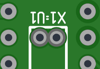
My most recent submission includes an area where I need clearance between two plated holes and solder mask, too. I almost freaked out when verifying my PCB with the board viewer as it shows a grey area between the two pins. Consequently they look like connected to each other, which is not what was desired.
This is illustrated in the picture below:

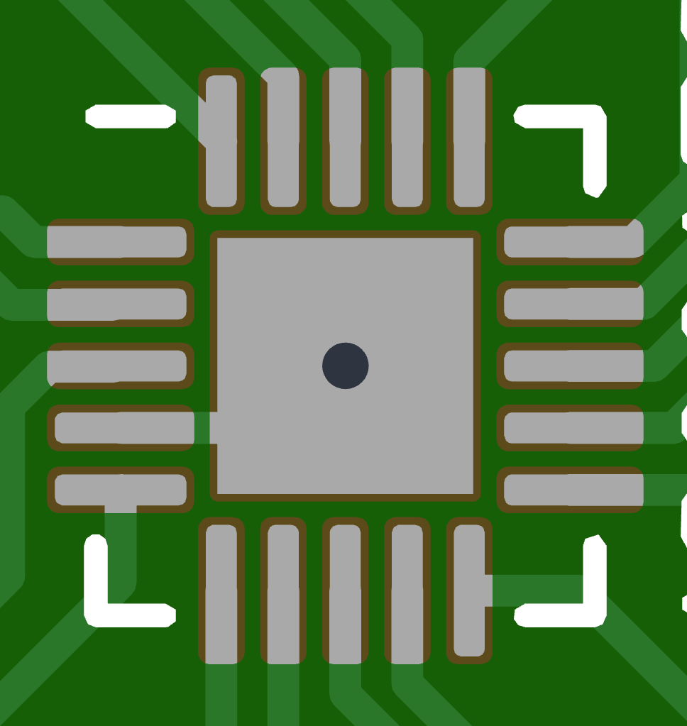
However, switching to the layer stackup view, I was relieved to see no copper between the two pins, as expected. See the picture below:

The area in question is in the centre of both pictures.
I believe the confusion comes from the grey-ish colour. From what I understand, this would indicate the bare board. May I suggest to use any colour but grey, for the reasons I have exposed.
Cheers,
V. C.
