Coplaner Waveguide Impedance testing

Standard 4 layer PCB has only mentioned single ended , Diff 90 and 100 impedance Trace width and space requirements.

This does not described Top or bottom Co-planer waveguide Trace width and Space from adjacent ground layer.

4 Layer 1.6mm ENIG Design Rules - :open_book: Knowledge Base / :magnifying_glass_tilted_right: Design Rules - AISLER Creative Community

RF trace need CPW as below stackup, while I get coupen test report when I place oder for standard 4 layer stack-up?

Hey @Ronak-Shah ,

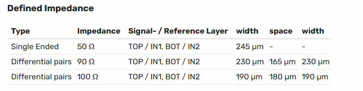
An impedance check can be requested. To do so, please request a quote for your project, letting us know what tolerance you require.
Compliance with the impedance values is then checked using a separate test coupon for each production run. All the different Z0 values for each layer are measured and recorded.

Does that help? :slight_smile:

Hi Sarah,

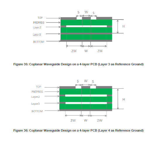
Can you share recommanded Width and Space for single-ended 50 Ohm Co-planer Trace requirment to meet 50 ohm +/-10 % Impedance on standard 4-layer Aisler PCB.

Then I will create layout with this W/S and while placing order, I will require CPW impedance testing .

Thanks,

Ronak

Hey Ronak-Shah :slight_smile:

to receive recommandations for the impedance testing, I would recommend that you send an email to our support team: support@aisler.net

Thank you!

Sarah

This topic was automatically closed 12 hours after the last reply. New replies are no longer allowed.