Overview
The impact of copper distribution and the effects on manufacturability is a complex topic, in this article we try to break down the main effect at a high level. And how you can improve your design for better manufacturability.
Common Defects
The main defects of improper copper distribution are:
- Overplating leading to shorts between traces
- Laminate residue on the PCB
- Bending of the PCB
Overplating
The Term Overplating is used when too much copper is added to the PCB during manufacturing, this may even lead to shorts when two copper features like traces are placed close to each other.
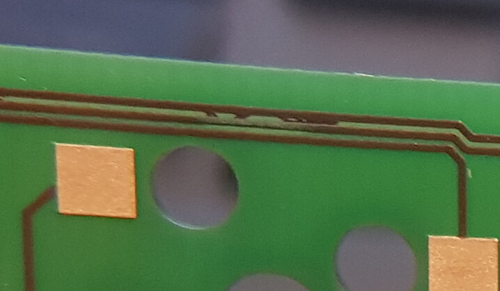
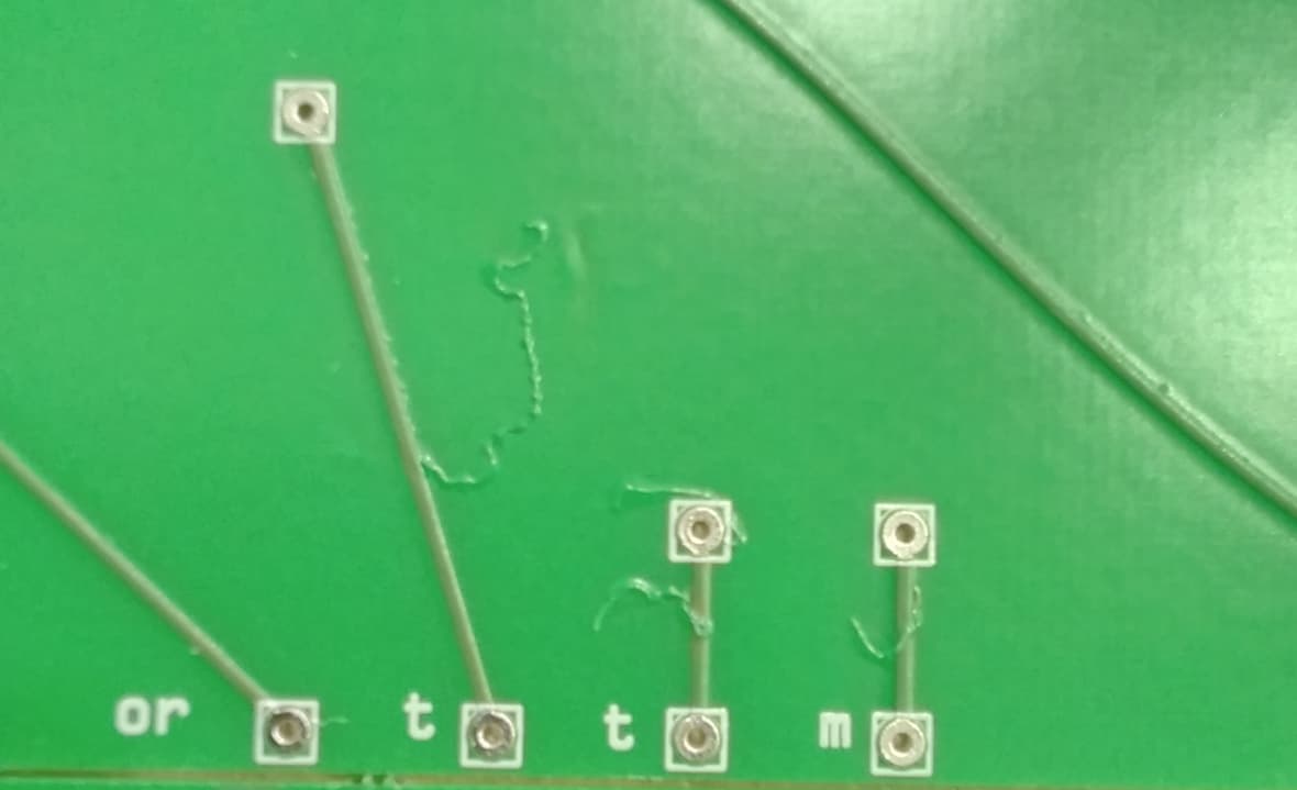
Laminate residue
During manufacturing, a laminate layer is placed on areas which shall not be plated, this laminate layer is later cleaned off. Poorly designed layouts can lead to strong overplating. The extra deposited copper creates a structure on traces that looks like a mushroom in a cross-section view. This structure traps the laminate, which cannot be cleaned off properly anymore.
Bending of the PCB
FR4 and copper have different temperature coefficients, if there is an uneven copper distribution, the parts with more copper expand and retract at another rate than an area with less/no copper. This will lead to bending, especially in thinner and larger PCBs.
Layout Design
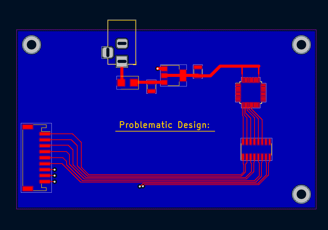
Problematic Design
Lets examine a problematic design example:
Only a small portion on the top side is filled with copper, traces run close to each other over a long distance, this may lead to overplating. The uneven distribution of copper between the top and bottom sides can result in board bending, particularly with thinner and larger boards.
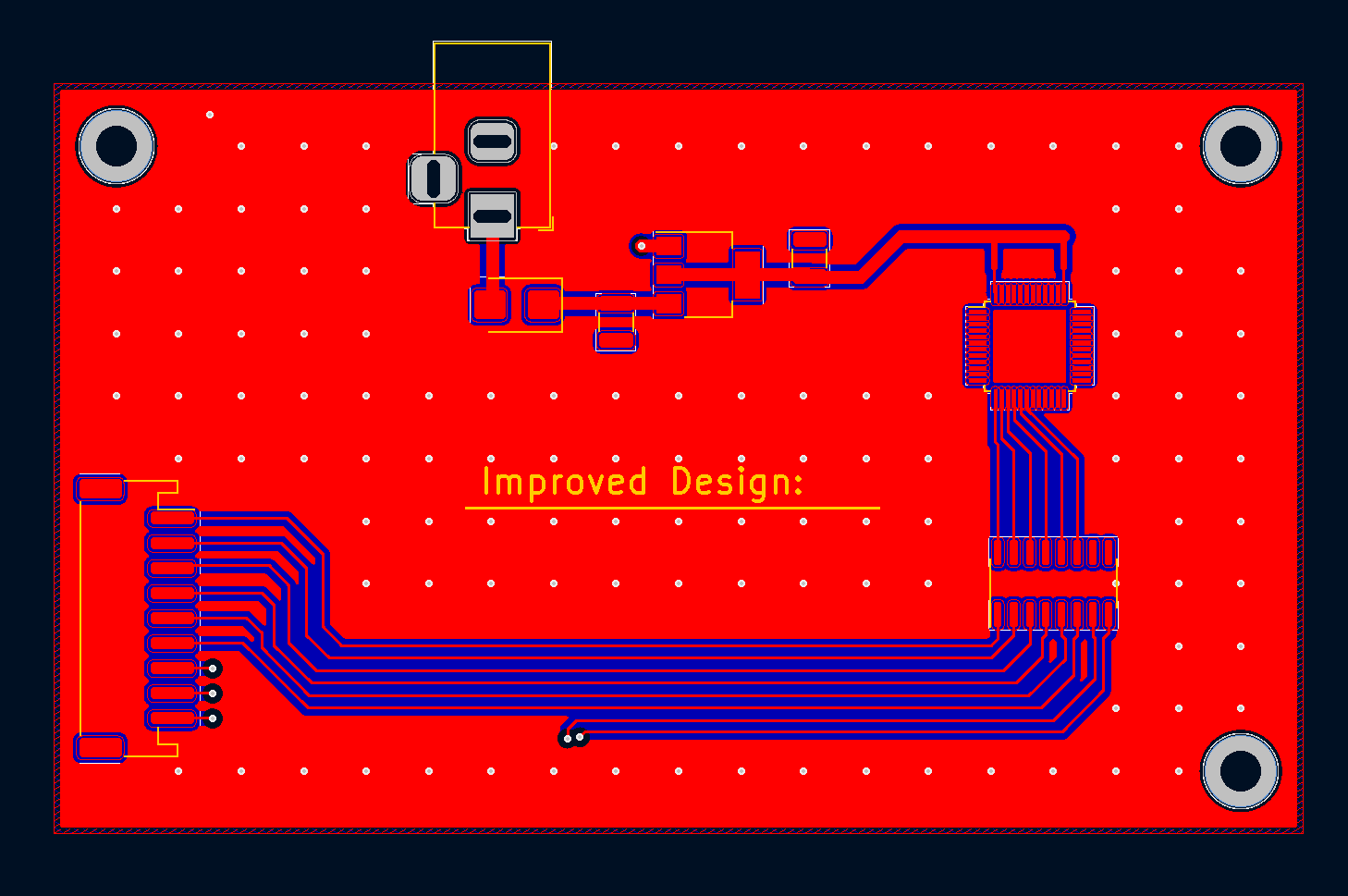
Improved Design
To improve the design manufacturability, a copper plane has been added on the top side and the distance between traces has been increased. The even copper distribution allows for even plating.