Hello everyone,
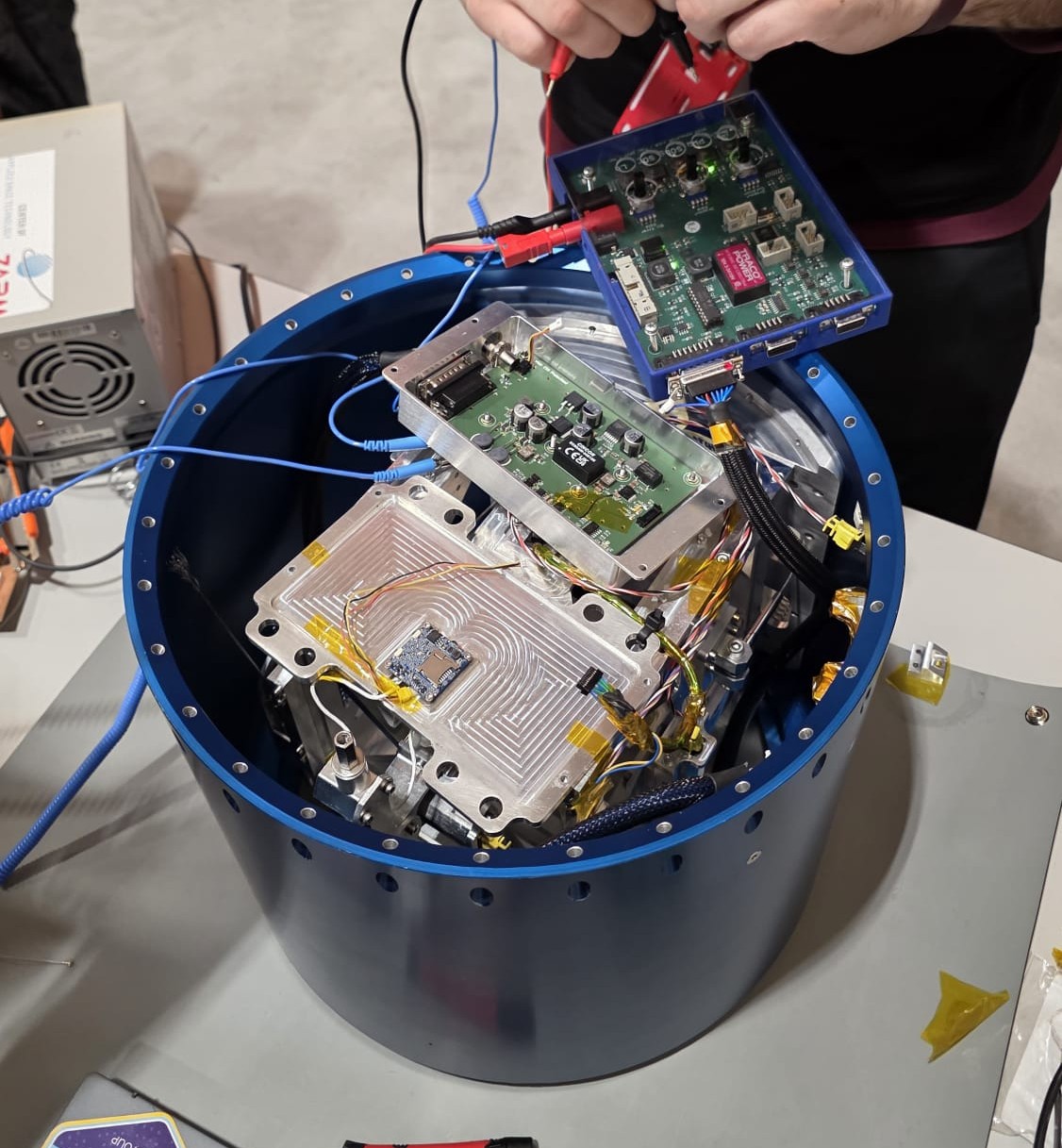
We are team HARTS from Slovakia, and we were designing the experiment of a hybrid heatshield intended for space vehicles re-entry into the atmosphere as part of the REXUS sounding rocket programme. We ejected our experiment capsule (FFU) at an altitude of 75,3km from the rocket. For more overall information about the project, please read our topic about our overall campaign. This section is entirely about our PCBs, which we designed and have been manufactured for us by AISLER through sponsorship for which we are very thankful.
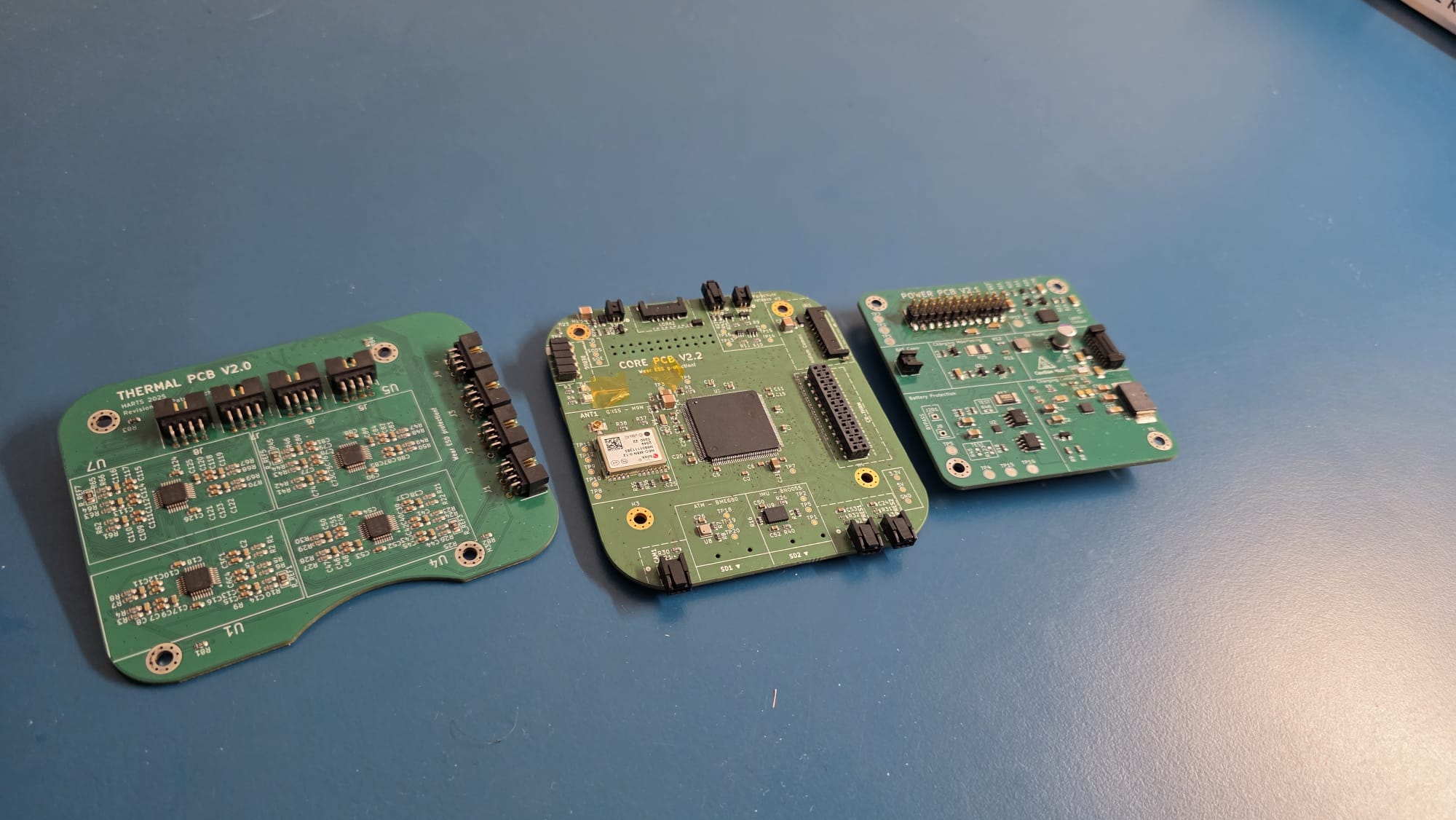
From an electronics standpoint, the architecture follows a modular approach with four dedicated PCBs: RMU, Power, Core, and Thermal. This separation allows us to isolate power, digital processing, and sensitive analog measurements while maintaining a clear and robust signal flow across the system.
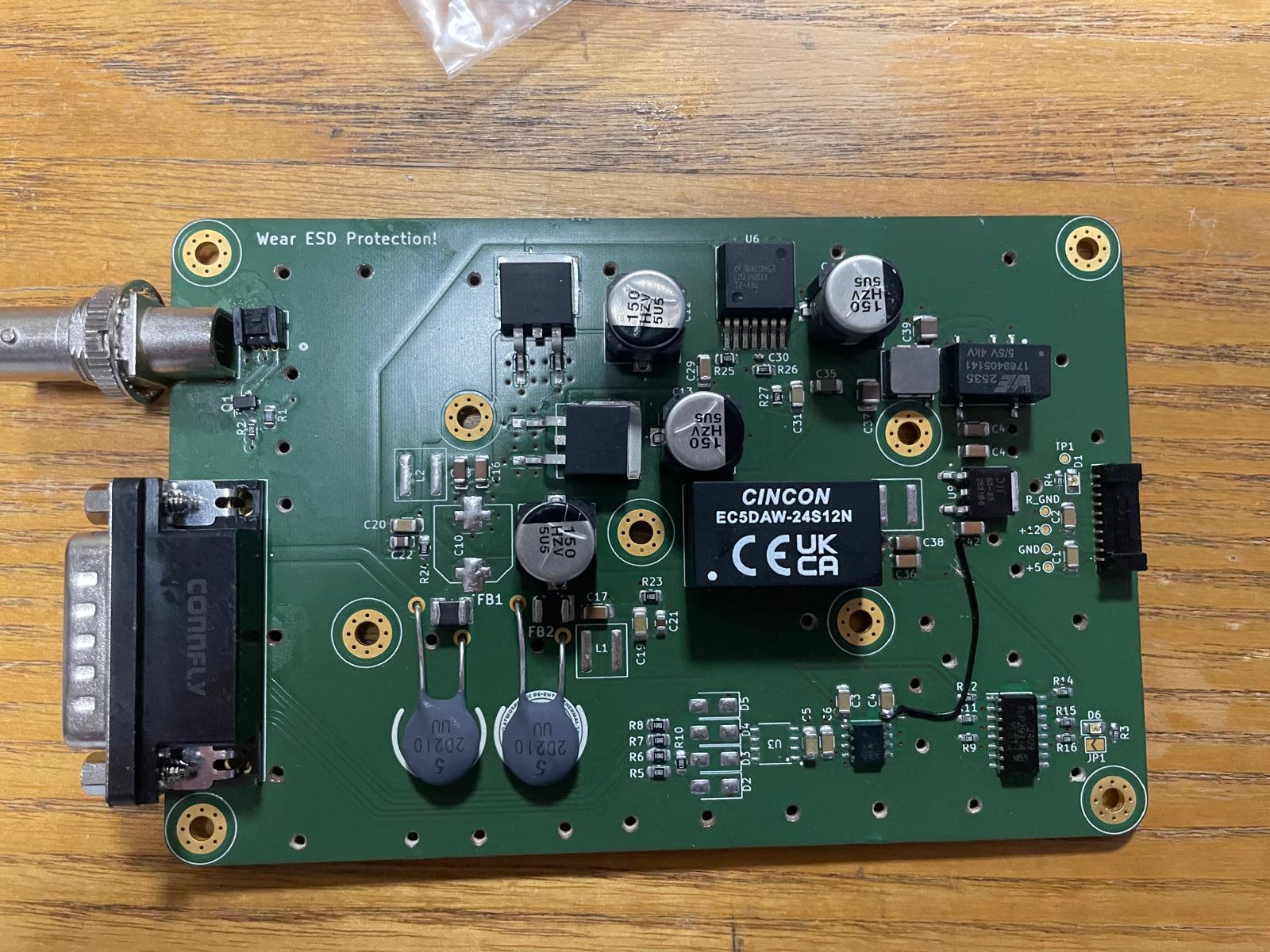
RMU PCB (Rocket Mounted Unit PCB)
The RMU PCB acts as the interface between the rocket and the experiment. It is the entry point for all external signals and power, and therefore plays a critical role in system robustness.
Its main responsibility is not just routing, but conditioning and protecting incoming signals before they propagate deeper into the system. The board handles power conversion from the rocket’s 28V supply and prepares intermediate voltage rails used downstream. Communication is also adapted here, ensuring compatibility between rocket systems and internal electronics.
Key aspects include:
-
28V input from rocket converted down to 12V, 5V, and 3.3V rails
-
RS422 to RS485 communication conversion
-
Galvanic isolation of critical control signals (LO, SOE, SODS) via optocouplers
-
Integrated camera module (RunCam Split 4 V2) for ejection monitoring
-
Configurable grounding strategy to mitigate noise between rocket and payload domains
A latching mechanism ensures that once the camera is triggered (via SODS), it continues operating independently after ejection. This board effectively bridges two very different electrical environments and was designed with noise, transients, and grounding issues as primary concerns.
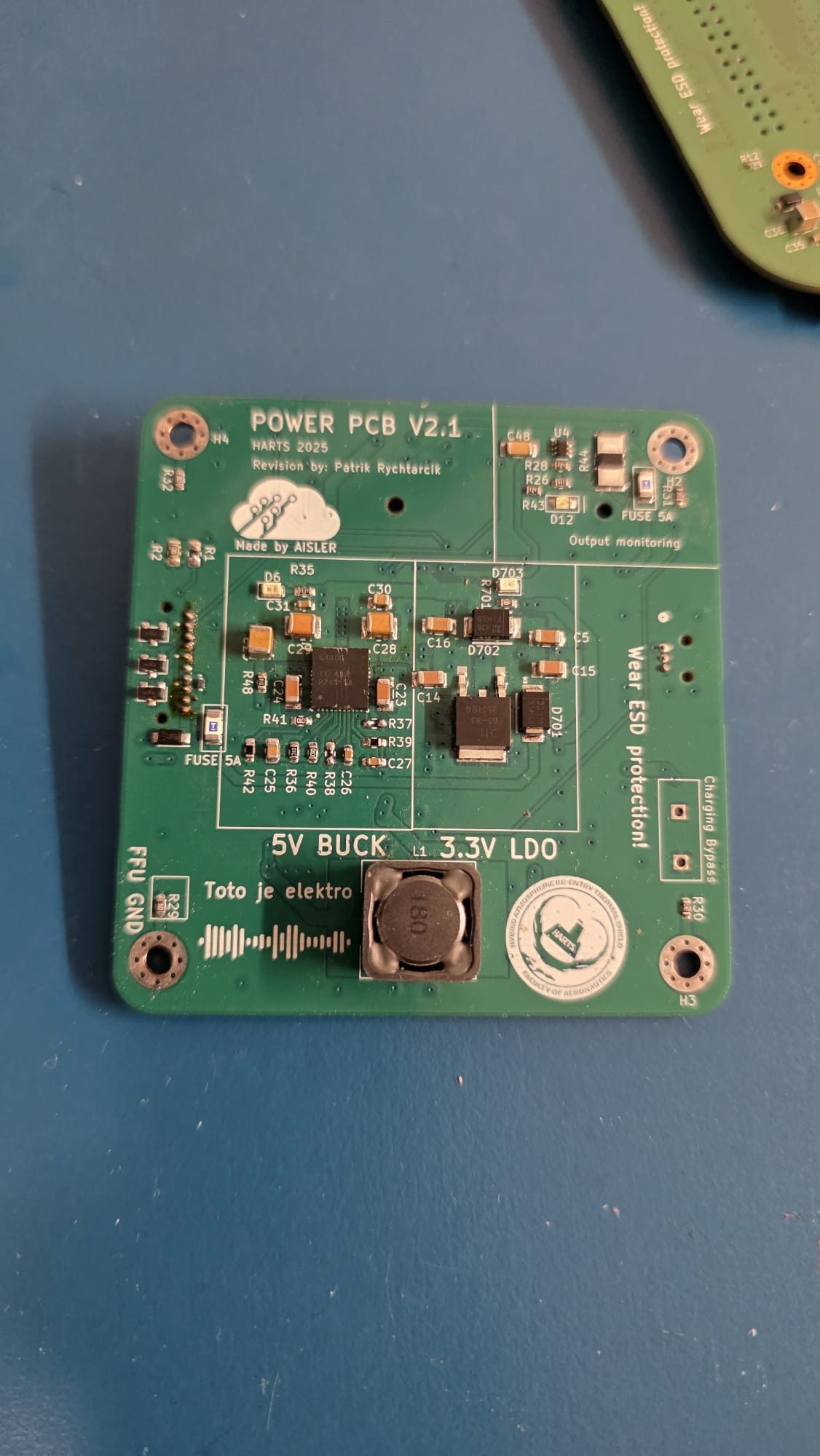
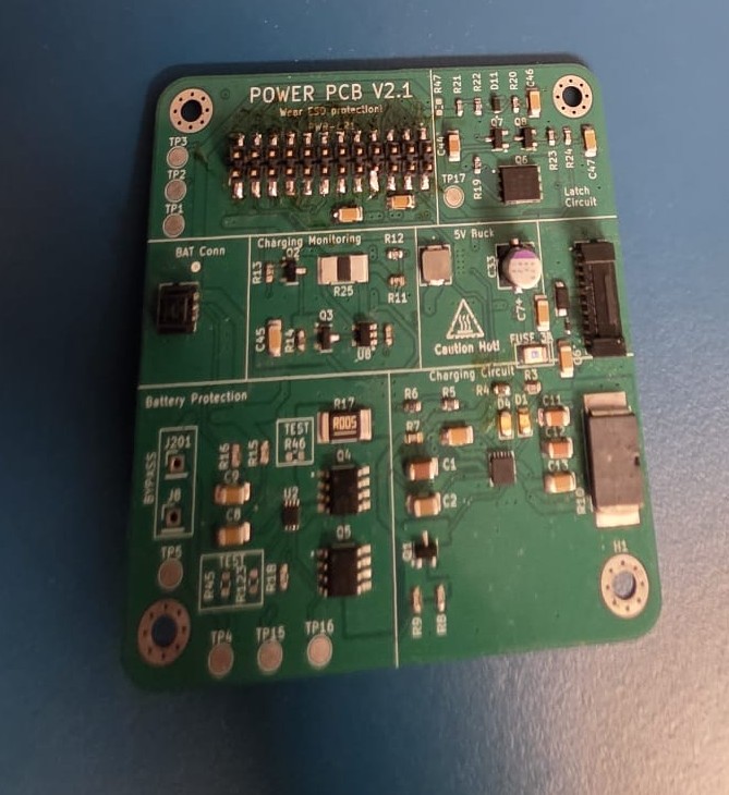
Power PCB
The Power PCB is designed to ensure the FFU operates safely and continuously, both while connected to the rocket and after separation. It manages energy storage, charging, regulation, and monitoring.
The system uses two Li-ion cells in series, forming a compact and efficient internal power source. This allows the experiment to remain operational even after complete disconnection from the rocket.
Key features:
-
2× Li-ion cells (7.2V nominal) with CC/CV charging (8.4V / 670mA)
-
Integrated protection (overvoltage, overdischarge, overcurrent)
-
Multiple regulated rails:
-
12V via boost converter
-
5V via buck converter
-
3.3V via LDO
-
-
Battery voltage and current monitoring for mission-critical decisions
-
Hardware latch circuit to maintain power even in case of MCU/software failure
A major design driver here was reliability. The latch circuit ensures that even if the Core PCB crashes, the system does not lose power. This is particularly important for recovery and parachute deployment logic.
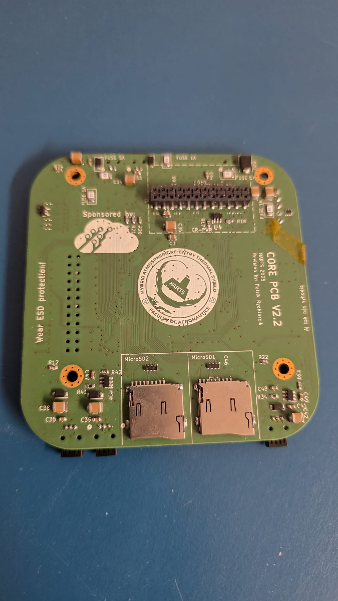
Core PCB
The Core PCB is the central processing unit of the FFU and coordinates all system operations. It is built around an STM32U575 microcontroller and serves as the hub between all subsystems.
It handles everything from data acquisition to communication and system health monitoring, effectively acting as the “brain” of the experiment.
Key responsibilities:
-
Telemetry and telecommand handling
-
Data processing and storage
-
Health monitoring and system diagnostics
-
Timing and experiment control
-
Interface to Thermal and Power PCBs
From a design perspective, the Core PCB is treated as a modular embedded system. Protection elements such as TVS diodes are used extensively, and attention is given to decoupling, clock stability, and signal integrity. The layout is still under iteration, with a focus on clean separation between digital and analog domains and minimizing EMI issues.
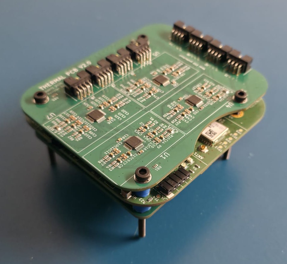
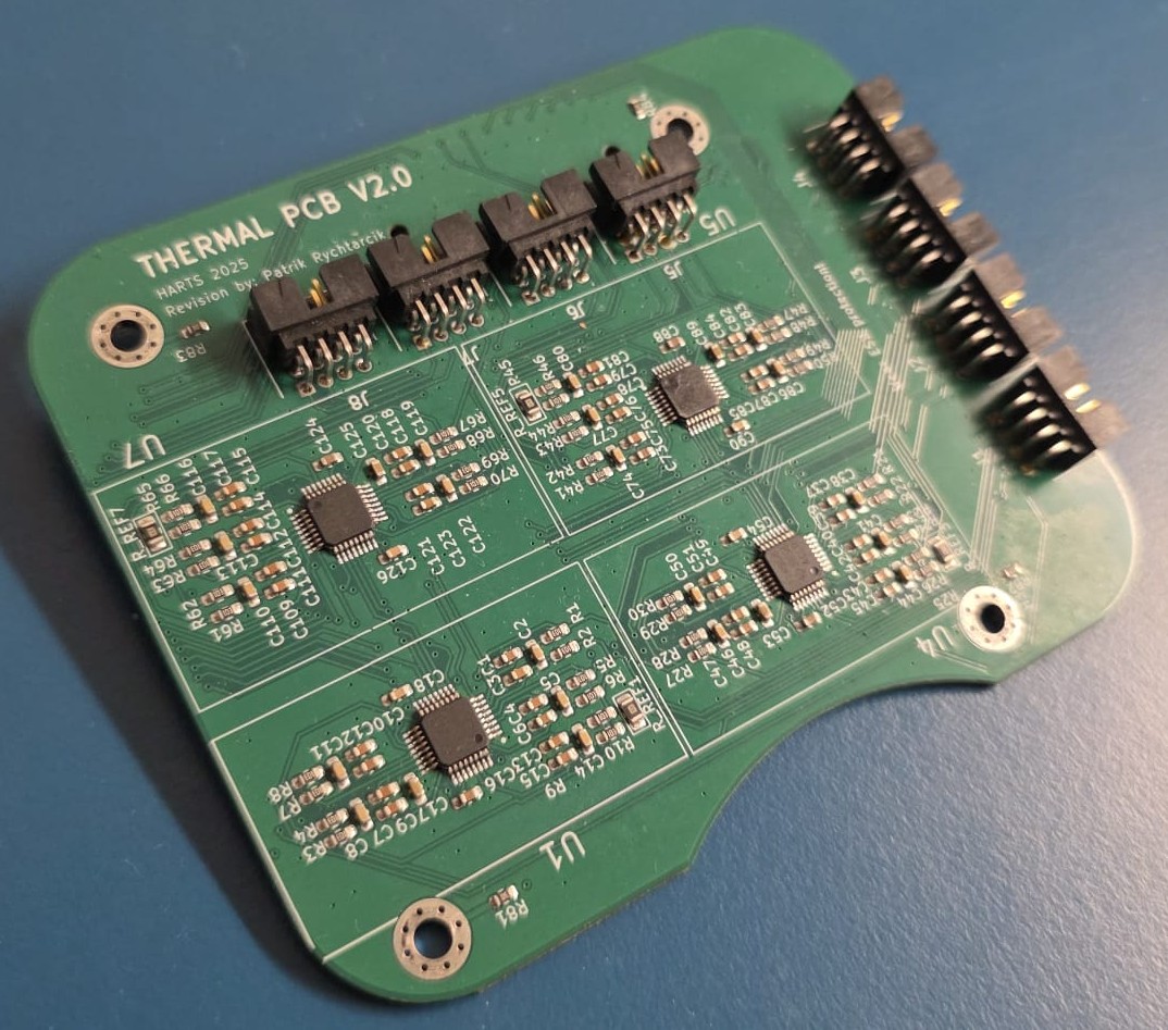
Thermal PCB
The Thermal PCB is a dedicated analog front-end designed for precise temperature measurements during flight. It interfaces with a large number of PT1000 sensors distributed across the heat shield and within the capsule.
The goal is to reconstruct a spatial temperature profile of the heat shield under real flight conditions, which places strict requirements on measurement accuracy and noise performance.
Key elements:
-
40 PT1000 sensors (37 on heat shield, 3 internal)
-
Multiplexing architecture to handle large sensor count
-
Signal conditioning (filtering and amplification) before conversion
-
High-resolution ADC with SPI interface to Core PCB
-
Precision reference circuitry for stable measurements
The design prioritizes low-noise analog performance, with careful component selection and layout strategies to reduce interference and thermal drift. Given the dynamic environment (vibration, temperature gradients), maintaining signal integrity is one of the main challenges.
At the end, we would like to give a big thank you to AISLER for sponsoring the PCB manufacturing for this project. Their support has been instrumental in enabling rapid iteration and bringing this design to life.