Hi Team!
I recently ordered a PCB that had a mid-mount USB connector. The PCB was automatically manufactured with a panel (nice!), however that same panel was getting in the way of the mid-mount connector.
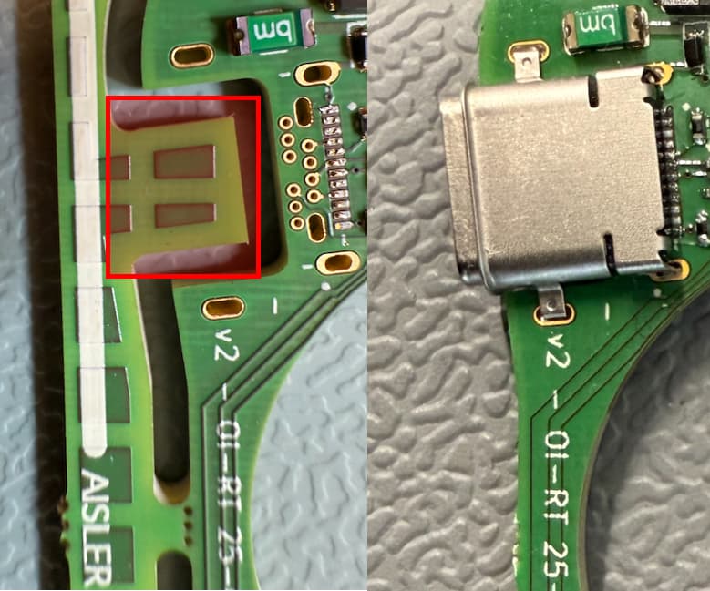
How can I ensure, e.g. using board outline, that the routing path will keep the cutout area clear?
Thanks for your help already!
In this case I would put keepout zone in the drawings for the pcb to advise that this “Must be free from Material”.
We don’t have an automated way of adjusting that design right now (June 2025) The current approach is to design a frame yourself.
This topic was automatically closed 12 hours after the last reply. New replies are no longer allowed.