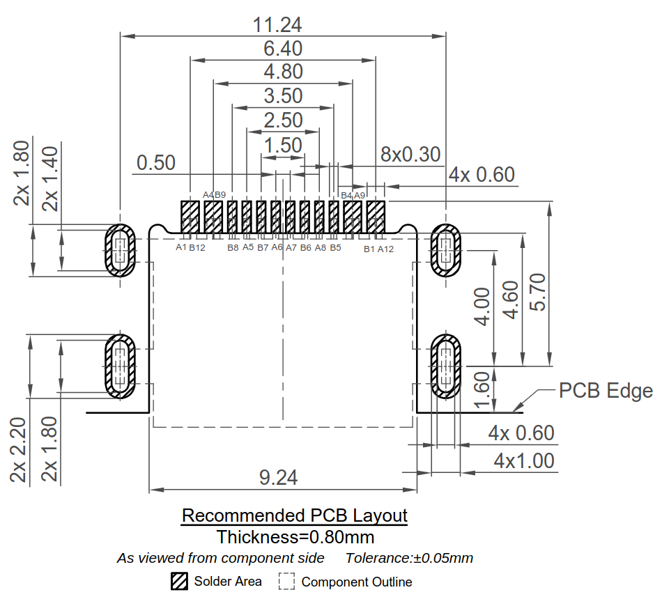
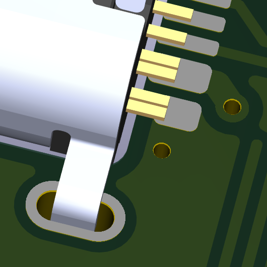
Designing the pads in a way to conform to the Aisler Design Rules (0.3 mm copper-to-edge clearance) results in a pin-pad overlap of only 0.2 mm, as seen in this screenshot (bottom pad adheres to the design rules, top pads according to connector footprint).
Is there any way around the 0.3 mm copper-to-edge clearance design rule in this case? Changing the mid-mount to a top-mount SMD connector would of course solve this issue, but my design greatly benefits from the center position of the mid-mount connector. Any other recommendations welcome as well. Thanks in advance!
We specify this rule so that copper features are not accidentally cut away, the 0.3 mm value is conservative. In cases where copper to edge is desired, you can ignore it. Please note that this may result in copper burrs, which you may have to manually remove.
Te elongated plated slots are more of an issue, our smallest tool diameter is 0.7 mm, if possible, increase the annular ring to 200 µm or more. This makes sure that the copper plating will safely attach. Due to the larger tool size, the connector sits more loosely on the PCB until it is soldered.