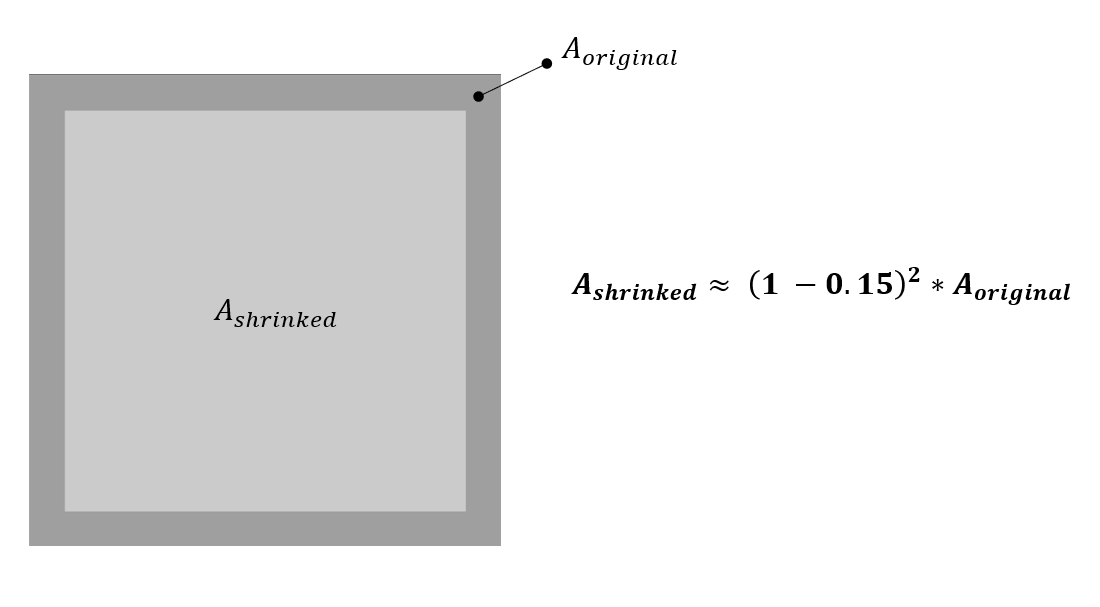
I usually put my own alignment holes in on the PCB and Stencil layers. However, lately I’ve found that the stencil holes end up significantly smaller then they should be. Namely, the holes that should be 2.45 or 2.50mm end up 1.9 or 2.0mm. Thus, I can’t use my solder paste stencil jig.
this means i also should not shrink my stencil openings for paste volume myself… but use the full pad area?!
(maybe this info is already stated somewhere in the specifications…)