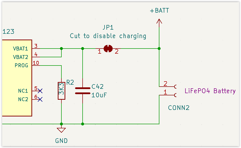
In my design, I have a LiFePO4 battery charger. In case the user decides to not use a rechargeable battery, it is possible to cut a jumper on the PCB so the charger cannot charge the non-rechargeable battery.
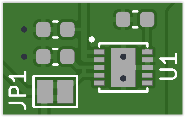
This is the footprint of such a jumper
When this design goes through the netlist check, it gives an error :
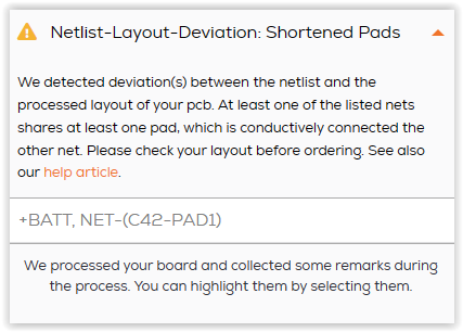
The message tells to highlight the error (I assume on the PCB render), but nothing happens…
How can I change my design to solve this warning/error ?