Hello Aisler Community!
Natnael Habtom developed a optimized GaN half-bridge at the Department of Vehicle Systems and Fundamentals of Electrical Engineering (FSG) at University of Kassel to demonstrate students the impact of parasitic loop inductance. Thanks to Aisler for the support during the design phase!
Below his short report:
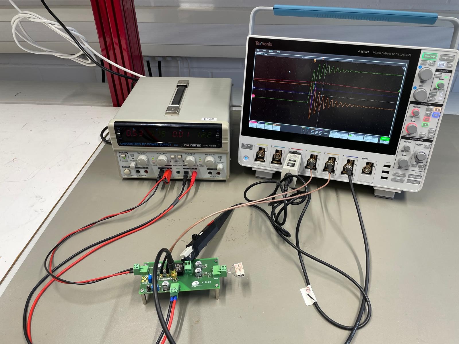
As part of my bachelor’s thesis, I developed a PCB design for a GaN-based half-bridge circuit. This project was designed as a practical demonstrator for educational purposes. It allows students to experience the theoretical concepts of parasitic effects in power electronics firsthand. Using a real setup of a GaN-based buck converter (EPC2307), we investigate how critically the PCB layout influences the waveforms of the drain-source and gate-source voltages, as well as the current dynamics.
I used the open-source software KiCad for the PCB design of the demonstrator. This allowed me to precisely create the complex 4-layer layout required to precisely implement the minimal loop inductances which are critical for GaN semiconductors within the layout.
A big thank you goes to AISLER for the excellent support. I ordered the finished layout through them and was impressed by the easy handling of the KiCad file upload as well as the very fair price-performance ratio. Thanks to the fast delivery and high manufacturing quality, the fine components could be assembled and soldered with high process reliability, which was crucial for the success of my project.
To minimize parasitic effects, the optimized design is based on a 4-layer stack-up. This is essential for minimizing loop inductance through large-area ground planes on the inner layers. Magnetic field cancellation between the closely coupled layers reduces commutation loop inductances and induced voltage peaks. This principle is vital for GaN FETs to achieve extremely fast switching speeds without destructive overvoltages.
The board was specifically designed to make parasitic elements visible during switching operations. To achieve this, the optimized design was contrasted with a deliberately suboptimal variant, where layout errors—such as artificially extended supply lines—were implemented via a separate carrier board. Subsequent measurement series documented significant differences: while the optimized layout exhibited very stable switching processes with low oscillations and overvoltages, the suboptimal variant showed significantly higher voltage peaks and pronounced ringing. These effects are particularly critical when using GaN semiconductors. Due to the extremely high switching speeds, even small parasitic inductances lead to oscillations that carry the risk of a “false turn-on” or can permanently destroy the sensitive gate insulation through overvoltages. Furthermore, ringing represents a significant burden on electromagnetic compatibility (EMC). These observations were validated by accompanying LTspice simulations, which confirmed that the additional parasitic inductance of the DC link is the primary cause of the degraded switching performance and the associated risks to component safety.
Due to its compact design and robust manufacturing, the board is ideally suited for use in power electronics laboratory courses. It provides an ideal platform to demonstrate the origin of switching losses and complex EMC issues in a practical way. Furthermore, the setup allows for a detailed investigation of the high switching speeds of GaN semiconductors. In this way, students can develop a deep understanding of the dynamic behavior and the specific layout requirements of modern wide-bandgap materials.