Abstract
This circuit appnote describes how one can export their PCB design without silkscreen layers from various EDA tools.
Including:
- KiCad
- Target3001!
- DipTrace
- Easy-PC
Introduction
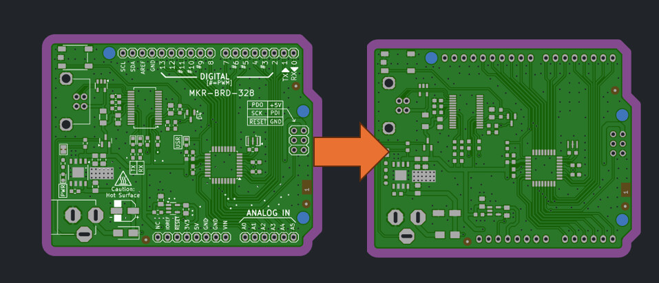
One might want to order PCBs without silkscreen for aesthetic reasons or lower cost by reducing steps during manufacturing. As we do not provide an option to deselect layers in the order process, it is required to send us the manufacturing data without the silkscreen layers.
This guide describes the process of exporting your design from the various EDA tools without the silkscreen layers.
Note: Ordering prototype PCBs without silkscreen does not effect the price, as the PCBs are manufactured on a shared panel with other PCBs that may have silkscreen markings.
The price can be lower when requesting larger quantities through a custom quote.
As with other digital media, it is important to make a backup copy before making changes.
KiCad
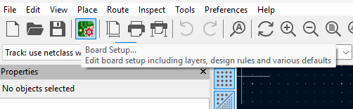
To disable the silkscreen layers in KiCad, we first head to the Board Setup. Locate the small PCB icon with a gear in the top left corner, or head to File -> Board Setup.
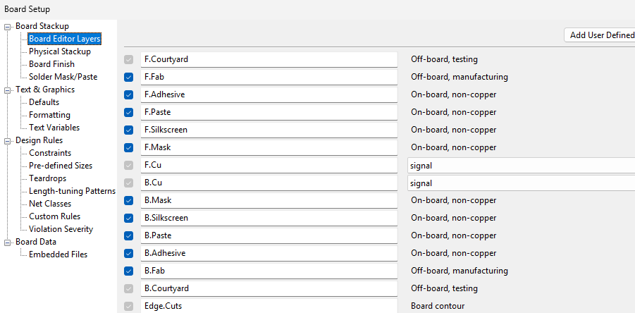
Uncheck the checkbox for the F.Silkscreen to disable the top silkscreen layer and B.Silkscreen for the silkscreen on the bottom side of the PCB.
Now click on Okay.
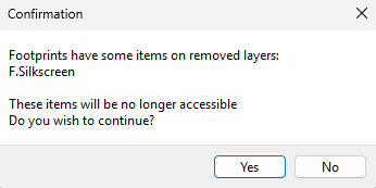
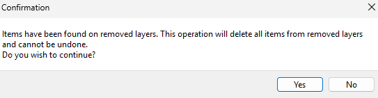
A warning will be displayed that footprints have features on the silkscreen layers that will now be removed. Since this is the desired action, simply select Yes.
If the silkscreen layers are desired later on, we can simply check the boxes to enable them again. This will restore all silkscreen within the footprint, including the designators.
Other features, such as drawings or text on the silkscreen layers, cannot be restored once the layer has been disabled. KiCad will warn you about this. Make a copy of your design and remove the silkscreen in this copied version if you require these features to be printed on a board later on.
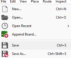
Select Yes if you want to proceed, now save the design using ctrl + s or via File -> Save.
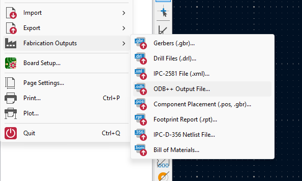
You can now upload your design by uploading the .kicad_pcb file directly, using our KiCad plugin, or by exporting the design as an ODB++ archive via File -> Manufacturing Outputs -> ODB++ Output File..
Target3001!
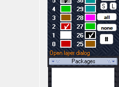
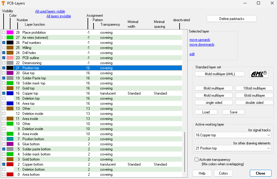
To disable the silkscreen layers in Target3001!, we first head to the PCB Layer Setup. Locate the “link” labeled Open layer dialog below the layer view on the lower right side.
This will open up the PCB-Layers setup. A default installation of Target3001! will use layer 21 for the top and layer 7 for the bottom silkscreen. Unfortunately, we cannot disable the layers but have to add another layer function. Thankfully, Target3001! allows for arbitrary layer functions.
Select the layer you want to adjust by clicking on it in the table on the left side, then use the edit “link”.
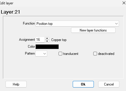
This will open up a small window in which the layer functionality can be set.
Select the New Layer functions button to create our disabled silkscreen layer.
Enter the new layer name in the text field on the top right of the window that is newly opened. For this demonstration we used the layer name top-silk-disabled but it can be any layer name that has not been used already or is bound to a specific function.
Then click on Add this layer function just beneath the text field and then Close.
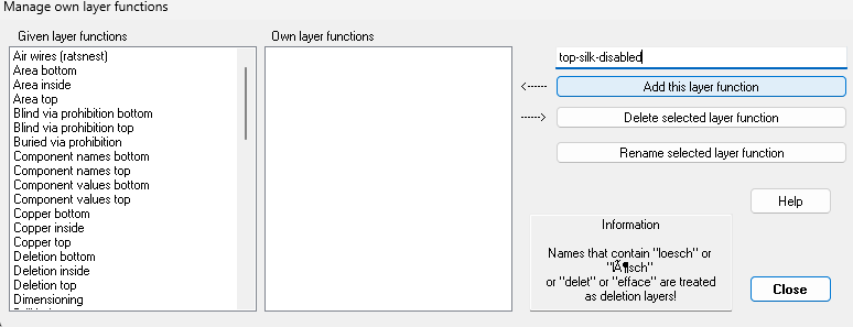
Then repeat these steps for all silkscreen layers you want to disable.
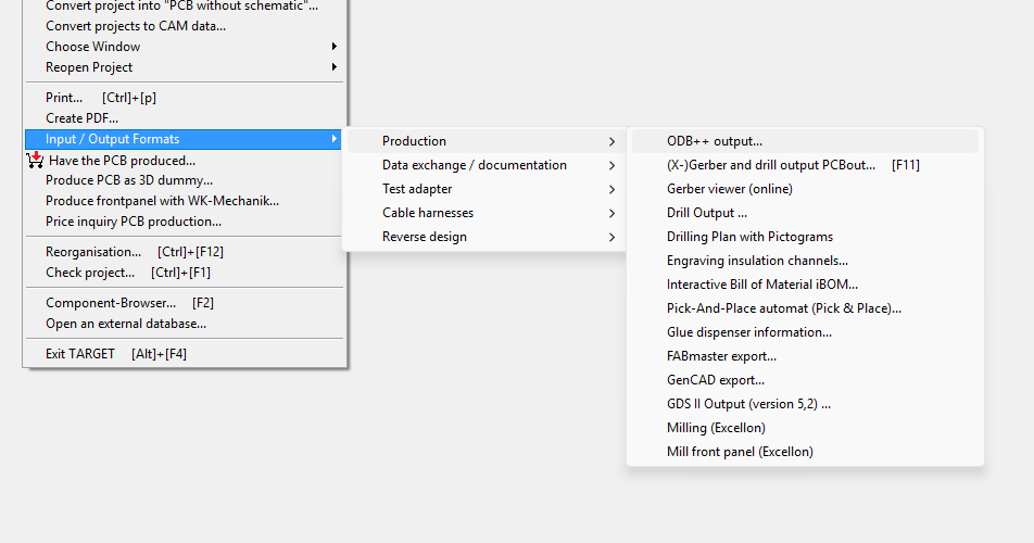
Close the other dialogs that are still open and save the file. You can now upload the *.t3001
file directly or export it as an ODB++ file.
To export the design as ODB++ head to File -> Input / Output Formats -> Production -> ODB++ output...
You can now upload this ODB++ file to our service.
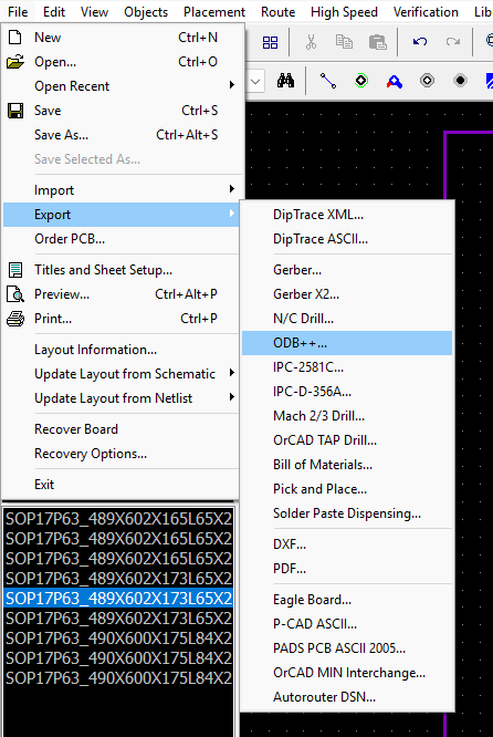
DipTrace
To export your design from DipTrace without silkscreen, you’ll have to use the ODB++ output functionality. Navigate to File -> Export -> ODB++ .
Now deselect the checkboxes for Top Silk and Bottom Silk, select approppriate values for the Solder Mask Swell and Paste Mask Shrink. Ensure that Make a Zip Archive is checked, then click OK to start the ODB++ export process.
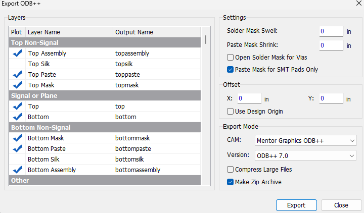
After the process is finished, simply upload the *.zip file.
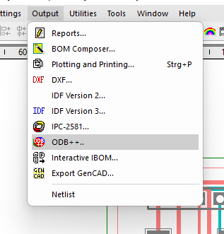
Easy-PC
Adjusting the ODB++ output to exclude the silkscreen layers in Easy-PC is quite simple.
First navigate to Output -> ODB++ in the PCB editor.
Now deselect the checkboxes for Top Silk Screen and Bottom Silk Screen the other options can be left as is. Click OK to start the ODB++ export process.
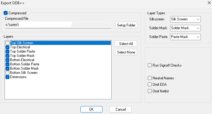
After the process is finished, simply upload the *.tgz file.
IMPORTANT NOTICE
AISLER assumes no liability for design assistance provided by this appnote. Engineers/designers are responsible for their design.