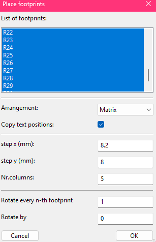
The Place Footprints plugin in KiCad is useful when multiple components need to be placed with a defined spacing and a regular pattern.
It can be used for different arrangements, such as:
-
Matrix
-
Linear placement
-
Circular placement
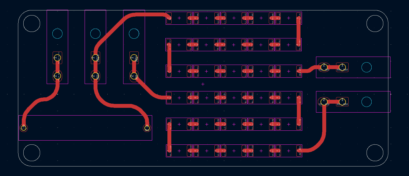
This is especially helpful for repeated components like resistors, LEDs, test points, or connectors.
After selecting the required footprints in the PCB editor, open the Place Footprints plugin.
In the plugin window, choose the arrangement type and define the spacing. For a matrix placement, the most important settings are:
-
Step X: distance between footprints in X direction
-
Step Y: distance between footprints in Y direction
-
Number of columns: number of footprints per row
-
Copy text positions: keeps reference/value text positions consistent
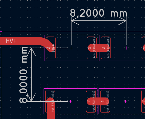
The distance entered in Step X and Step Y is measured from the center/origin of one footprint to the center/origin of the next footprint.
It is not the distance between pad edges, component outlines, or courtyard borders.
Recommendation
Before placing the footprints, check that:
-
the correct footprints are selected
-
the footprint origins are correct
-
the X/Y spacing is known
-
the selected arrangement matches the intended layout
-
clearances are checked after placement
-
DRC is run after the layout update