Plated and Non-Plated Holes

TL;DR

  • We interpret drill diameters in your CAD data as final hole diameters (endsize).
  • Drill diameters will be adjusted to available tool diameters.
  • The minimum drill distance should be at least 0.25 mm (edge-to-edge, tool diameters)
  • The minimum distance between NPTHs and copper structures should be at least 0.25 mm.
  • The maximum final hole diameter of PTHs is 5.65 mm.

About this article

To realize the drills on your PCB as close to your CAD data as possible, we must adapt them for the manufacturing process. This includes the adjustment of diameters and - in some cases - also their removal.

This article explains how we process your data. It serves to prevent common questions and misunderstandings and will help you to create a robust PCB design.

Final hole diameter

Please note that we interpret any drill diameters in your CAD data as final hole diameters (endsize).

The manufacturing including selection of the appropriate tool diameter (including tool and copper compensation) is our job. You don’t have to worry about that.

Adjusting to available tools

We cannot manufacture every diameter, as the number of available tools is finite.

Our tools have a graduation of 0.05 mm for diameters < 2.0 mm (1.95 mm, 1.90 mm, 1.85 mm…) - for larger diameters, a graduation of 0.1 mm (2.10 mm, 2.20 mm, …).

For the preparation of the production data, we select for each hole the tool diameter that is closest to the desired hole diameter.

Since our largest tool diameter is 5.8 mm, we automatically convert larger drills (without adjusting the diameter) into inner millings. As milling is performed after the copper plating process, PTHs can be manufactured with a maximum diameter (final hole diameter) of 5.65 mm.

Removing overlapping and very close drills

In order to avoid drilling fractures during the manufacturing process, all drill holes must maintain a minimum distance of at least 0.25 mm (0.001 in).

The minimum distance here refers to the tool diameter! This can lead to a situation where drills in your drawing (endsize) meet the minimum distance but fall short of it after we select a larger tool diameter.

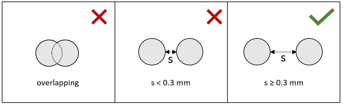
Important: Holes that do not comply with the minimum distance must be removed by us and will no longer be displayed by the BoardInspector. (We are currently working on marking such changes more clearly visible.)

Compensation

Here we must distinguish between two different types of (circular) holes: Plated through holes (PTH) and non-plated through holes (NPTH).

Copper plating always reduces the effective diameter of a drill hole. Therefore, it is necessary to choose a larger tool diameter for PTHs. NPTHs also experience an - albeit smaller - increase in diameter to account for tool wear.

tool diameter = final hole diameter + compensation

compensations:

  • Plated through holes (PTHs): 0.15 mm
  • Non-plated through holes (NPTHs): 0.05 mm

Copper Cropping

To prevent NPTHs from being unintentionally plated through, no copper must be present within the hole and/or in the immediate vicinity. Even small copper fragments in the copper layers can lead to an accumulation of copper in the hole due to the production process.

To avoid unintentional through-hole plating, we remove all copper from the copper layers that are within the drilling circle and a distance of 0.25 mm around the drill hole.

So please make sure that traces, pads or other copper structures keep a minimum distance of 0.25 mm to NPTHs.

1 Like

Hey @christina,

could you please add the Via Plating Thickness? (Or generall copper plating thickness) :thinking:

I guess this fits here. Thank you so much :smiley:

Hi Andreas,

The general copper plating thickness is approx. 18 µm. (It’s the difference between the min. processed copper thickness and the base copper thickness.) You can find it `here or in our stackup information.

Best regards,
Manuel

I would like to have small VIAs in a PTH mounting hole’s pad for better mechanical stiffness.
1.6mm hole, 3mm pad diameter and I would like to put 0.2mm VIAs into that pad like this:

Your tool removes it however i kept 250um from hole edge to hole edge.
How much space do I need to keep?

image

Hi @effectbakro ,

the minimum distance refers to the tool diameter. According to the dimensions of your drills

  • center drill (endsize: 1.6 mm → tool diameter: 1.75 mm)
  • circular drills (endsize: 0.2 mm → tool diameter: 0.3 mm)

you’ll have to keep a distance (edge-to-edge, center drill - circular drill) of at least 0.25 mm + 0.15 mm / 2 + 0.1 mm / 2 = 0.375 mm.

Cheers,
Manuel

Hello @Manuel-from-AISLER ,
can you clarify why you use two different compensation values for the 1.6mm and 0.2mm vias (plated holes).

According to the articele above the compensation value for plated holes (and therefore also vias?) is 0.15mm. I assume that this applies to both hole types.

So why is the tool diameter for the circular drills 0.3mm and not 0.35mm

Thanks in advance!

Hello,
I had an issue with elongated plated through holes on my last PCB (2-layer, complex). The PCB was correctly displayed with the appropriate holes, but they are missing in the manufactured PCB. As I understand it, plated slots are possible with complex design rules. Are there any hole size rules that I have overlooked? The hole size is 3.1mm x 0.8mm.

Thanks in advance!
Frederic


Hi @holzi ,

First of all, I would like to apologise for the late feedback.

Unfortunately, it is not clear from the main article that, with a few exceptions, through-plated holes with a diameter smaller than 0.5 mm (usually vias) are not copper-compensated. The nominal diameter is then drilled - if available - with a tool diameter of the same size. The background to this procedure is the assumption that such small holes have the only function of creating a conductive connection. In this case, a tool diameter that is not increased has a positive effect on the manufacturing reliability of the vias (ratio of pad size to tool size). A plated-through hole with a target diameter of 0.45 mm is thus drilled with a 0.45 mm drill. As I said, however, there are exceptions to this. A hole < 0.3 mm (e.g. 0.2 mm) on a complex classified board is currently drilled with a 0.3 mm drill, as this is preferable in terms of production safety (breakage of the drilling tool). The diameter adjustment of 0.1 mm is therefore not the result of a copper compensation, but of a tool adjustment. In the end, however, this hole will have a diameter of about 0.2 mm.

I have to say at this point that the issue of tool selection for manufacturing is actually our concern, not the customers’. I will therefore consider whether in future we should relate the minimum hole spacing (which currently refers to the tool diameter) to the nominal diameter. That should make a lot of things easier.

Best regards,
Manuel

1 Like

Hi @frederic-krause-rwth ,

Apparently we have a problem here with the way the elongated holes were drawn by Altium (some unsupported macro). The holes could not be prepared correctly for manufacturing. I’ll look into it and then we can manufacture the boards again. I’ll come back to you directly!

Update (30.01.2023): The bug has now been fixed!

Best regards,
Manuel

@Manuel-from-AISLER Thank you for looking into the issue!

Hello @Manuel-from-AISLER

Thank you very much for the detailed reply. Maybe a lookup table for the smaller via diameters is a possible solutiong to this issue.

Please note, that the tooling diameter may be of interest for other topics than via to via distance also. In example for RF applications typically the outer diameter (tooling diameter) of the cylindrical via structure is of interest (skin effect).

Tooling diameter values of the smallest via sizes are sufficient (e.g. 0.2mm, 0.25mm, 0.3mm, 0.35mm, 0.4mm).

Thank you very much! The ability to communicate on this platform so easily is simply awesome!

Hello Manuel,
I have an issue with my design “AutomationCarrier Projekt: ZJWLVMBB”
The board inspector complains about the drill distance of many vias. E.g., case #1 are two 0.3mm vias with 0.625mm center to center distance. According to your replies “diameter smaller than 0.5 mm (usually vias) are not copper-compensated”. So what is the issue??

Best regards,
Sven.