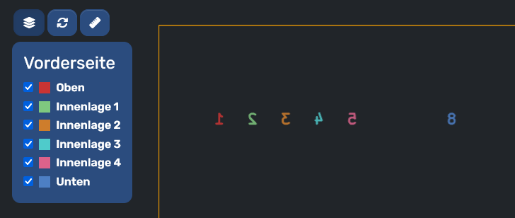
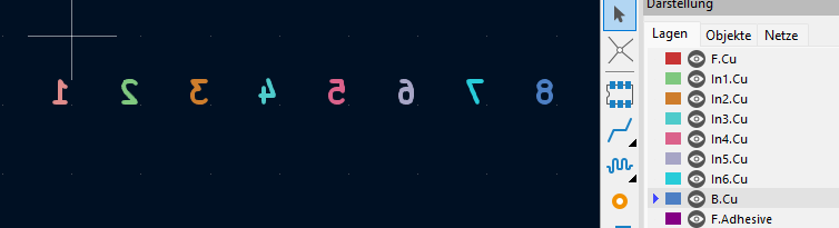
I use KiCad 9.0.5 and made a 10cm*10cm PCB with the letters 1 2 3 4 5 6 7 8, one letter per layer.
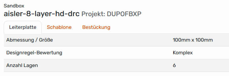
I used the provided 8-Layer example from Aisler as you can see in the name of the Project.
F.Cu has the letter 1,
in1.Cu has the letter 2
in2.Cu has the letter 3
etc…
But the board does not get recognised as a 8 layer board.
Kicad:
Aisler:
PCB Viewer: