I am still new here so I believe am missing something very obvious.
I created, ordered and received a simple PCB (RP PICO + an extra module), yet my idea was having filled ground zones on front/back areas. For this particular project it doesn’t matter so much, but if I’d need some signal traces, then this is an issue.
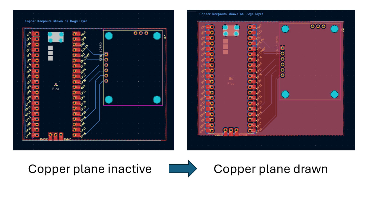
Using KiCad I added filled zones to the front and back copper layers, but the PCB arrived with apparently no copper layer except the traces (so - no fill)
I checked the files you sent us pre-processing, and they did not contain copper planes, so we can rule out an error on our side. Additionally, I also took a look at the KiCad files you shared on Bitbucket. There you’ve added planes, but they are not “active”, you need to use click b on your keyboard to refresh/draw them. You can undo the action by pressing ctrl + b but you always need to refresh the copper planes and the run the DRC before submitting your file for manufactruring.
I also noticed the text “copper keepouts in Dwgs layer”, please note that we do not manually adjust your design files. To offer our prices, we only do some automatic processing. If you require these keepouts, you can use the rule areas within KiCad after which you need to refresh the copper planes again.
Btw you can simply upload your KiCad PCB file; no need to generate Gerbers.
I hope this cleared a few things up. If you have further questions I am happy to help.