Overview
SoMs or System on Module allow to quickly add subcircuits to your design and save development time and complexity. Just like any other component, they need to be set up correctly for a successful assembly. But we’ll focus on the intricacies of working with SoMs in this article specifically.
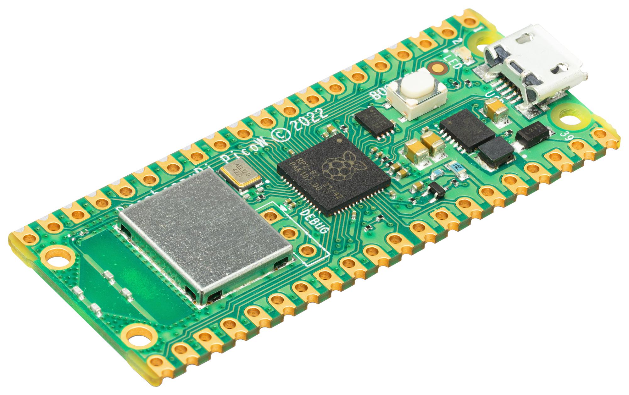
SoM with castellated Edges
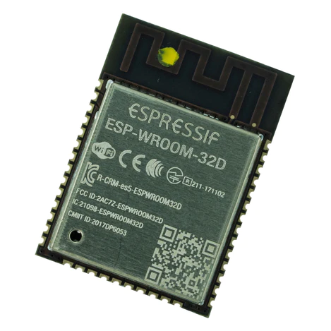
Simpler SoMs like microcontroller or Wi-Fi modules often utilize plated side contact, so-called castellated edges, they allow the SoM to be directly soldered to the custom PCB. This provides the advantage that no additional connectors are needed, which lowers the cost and complexity. An additional benefit of castellated edges over other processes is the ability to inspect the solder connections using automated optical inspection.
Design Workflow
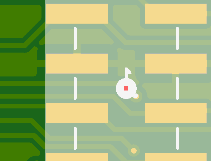
When creating a footprint for such a castellated module, it is important to dimension the stencil aperture large enough to provide enough solder paste to wet all flanks sufficiently. Reputable manufacturers will provide example footprints.
Do not use a mixed SMD/THT footprint for castellated modules, the solder paste will flow into the holes resulting in insufficient soldering results.
Specify the full SoM part number in your CAD library, don’t use the product description. Only so is our BOM tool able auto-assign it. If you leave out parts of the MPN, you may need to manually search it within our tool.
An example: Don’t specify Raspberry Pi Pico W but SC0918.
After you assigned the components, head over to the assembly tab, the 3D shape marking the SoM should include all pads, also check if the location of the first pin is correctly recognized.

Summary
- Use the recommended footprint.
- Specify the full Manufacturer Part number.
- Check if we recognized the components placement and orientation correctly.
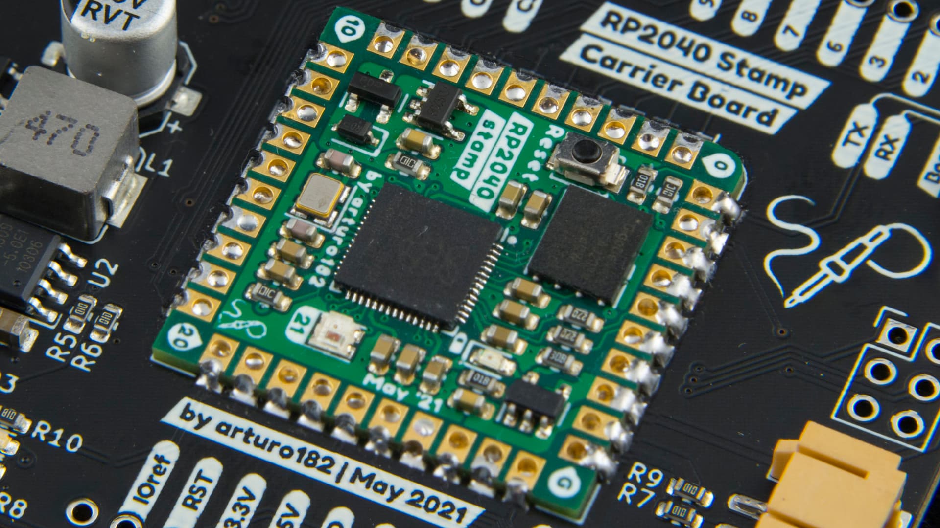
SoM with Mezzanine Connectors
SoMs with a high pin pitch or which need to be serviceable cannot make use of castellated edges, they instead utilize mezzanine connectors. The range of connectors varies from simple 2.54 mm pin headers to 0.6 mm pitch keyed and impedance controlled connectors.
Design Workflow
As SoMs with Mezzanine connectors require precise placement, designers tend to include all connectors in one footprint, by doing so, the spacing cannot be changed accidentally. Doing so, however, has the downside that the part number, position, and rotation of the individuals connectors are not included in the design file, which is required for assembly.
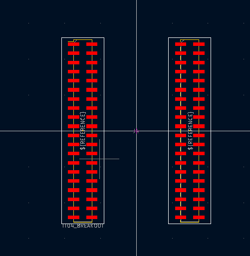
A better approach is to place all the connectors as individual footprints, then group and lock them in the PCB designer. Specify the full connector part number in your CAD library, don’t use the product description. Only so is our BOM tool able to auto-assign it. If you leave out parts of the MPN, you may need to manually search it within our tool. An example: Don’t specify Mezzanine-Connector, but MOLEX 87831-4029.
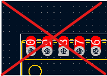
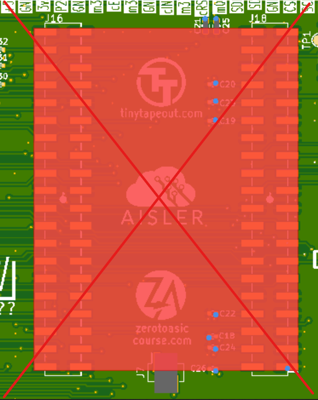
I can’t change my footprint, now what?
A crude workaround is to place a pseudo footprint in the centre of the connectors, this way the connectors appear in the BOM and the position is marked. Make sure to include the connectors and exclude the module footprint for assembly.
Contact our support before ordering if you make use of this workaround.
Summary
- Use the recommended footprint.
- Use Groups for the SoM connectors, do not include them all in one footprint.
- Specify the full Manufacturer Part number.
- Check if we recognized the components placement and orientation correctly.
- Only if unavoidable, make use of the workaround.