Smart Tests
With our Smart Tests we provide you with a detailed test report of your manufactured PCBs directly after production. Not only that: We compare the netlist based on your schematics with the final PCB layout and point out possible deviations even before you have placed your order with us. This gives you a great opportunity to identify and improve weaknesses in your design - even before production! This is smart!
About this article
This article explains everything you need to know about our Smart Tests.
- You do not understand the meaning of Processing Notes displayed after uploading your project?
- You have received a faulty test report and are now wondering what to do next?
- You are simply curious and want to learn more?
Then you have come to the right place.
Basics about E-Test
The high efficiency of today’s flying probe testers enables a complete electronic check of each individual board before it leaves the manufacturer.
The test procedure is always identical: For each measurement, two different measuring points are approached simultaneously by two probes. A voltage is applied, and the resulting resistance value is measured and documented.
But how does the flying probe testing machine “know” between which points to measure and how to interpret the results?
The basis for the test program is formed by the nets and pads defined in the respective PCB design, which are derived from the circuit diagram. They determine which points must be conductively connected and which must not.
Pad:
Pads are designated and exposed surface areas at which components can be soldered or mount onto the PCB.
Net:
A net is a group of pads that are conductively connected to each other.
The logical connection between nets and pads is hereby as follows:
All pads of a net must be conductively connected to each other. Conversely, pads from different nets must not be connected. This logically also leads to the fact that each pad can only belong to one single net.
During a test run, both pads of the same net and pads of different nets are approached. Our Smart Test checks for open connections or short circuits.
OPEN: The measured resistance value exceeds a pre-defined threshold for pads of the same net. This means the two pads are considered as not connected.
SHORT: The measured resistance value between pads of two different nets falls below a pre-defined threshold. Thus, the two probe points are considered as connected.
Which pads belong to which nets is described by almost all EDA applications in a separate file, the IPC-D-356 netlist.
IPC-D-356, Gerber and Processing Notes
Unlike the other PCB data, the detailed test specifications are not written and transferred in Gerber, but in a standardized IPC-D-356 format, or IPC netlist for short. We extract this file from any supported CAD file automatically when you upload your project.
Please note that we ignore any IPC file that comes from unsupported EDA-applications. If you want Smart Tests, please upload your CAD file, or follow the described upload method for supported EDA-applications. Please have a look here to see for which EDA-applications we support Smart Tests.
As already mentioned, the logical relationship between the listed pads and nets in the IPC file is based on the schematic in your CAD application.
For a meaningful test, it is therefore necessary that the schematic has also been completely implemented by the developer in the corresponding PCB design. Test data and PCB design should match before manufacturing.
When processing your project, we compare the nets (and pads) with the layout of you PCB. Should we find deviations, we will automatically display a corresponding Processing Note which will help you to figure out, whether this discrepancy is tolerable, or not.
Let’s take a look at the following example:
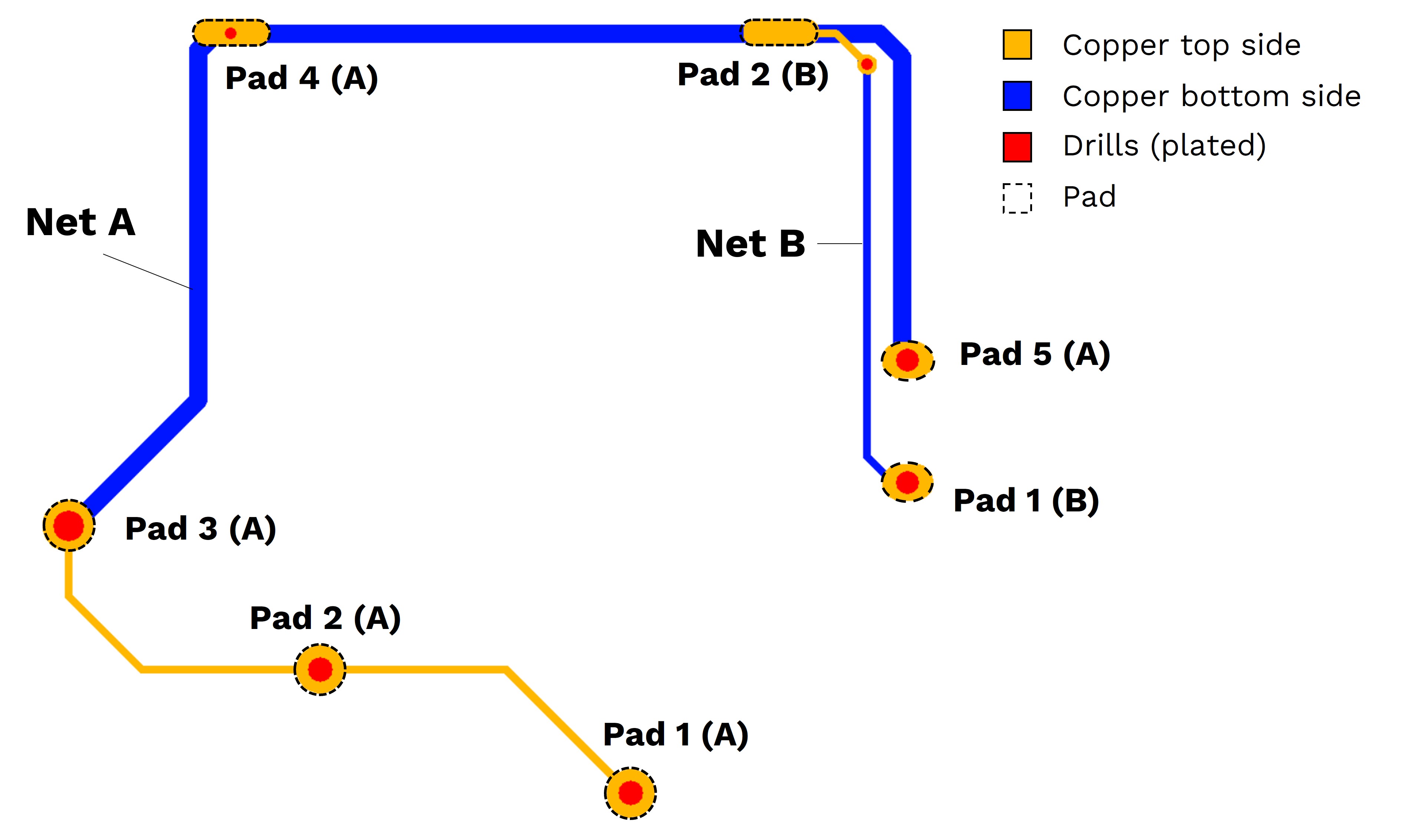
The graphic above schematically shows two nets (A & B) and their design on a 2-layer PCB. Net A contains five, Net B two pads. There are two separate copper structures, which are not connected to each other in any point. Each copper structure “includes” all the pads of one of the two nets. Netlist and layout match perfectly. If this layout is not realized in production as shown (due to a manufacturing error), this will be recognizable in the corresponding test results.
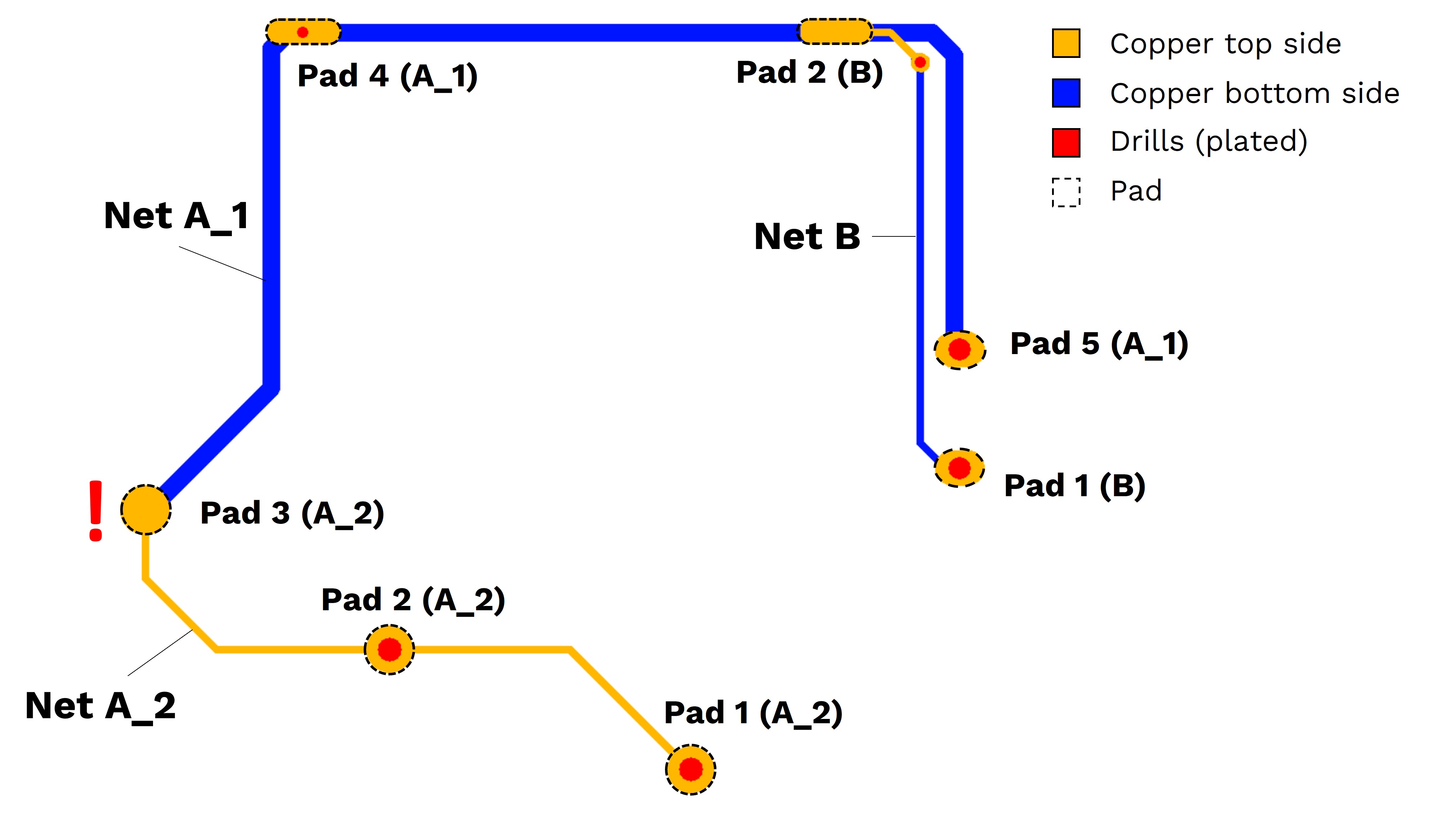
Case 1: Netlist-Layout-Deviation: Unconnected Pads
Let’s assume the plated through hole in Pad 3 of Net A is missing for any reason. This will disconnect the two conductors of Net A: The conductor on the topside ( with pads 1, 2 & 3) and the conductor on the bottom side (with pads 4 & 5).
In this case, our system will display the warning “Netlist-Layout-Deviation: Unconnected Pads” in our Board Viewer. We also display the name of the affected net – in this case “A”. Please check your routing/layout once again, unless this deviation is intended.
If you continue with your order without removing the detected deviation in your project, we will create two new nets for the E-Test. The nets A_1 and A_2 will replace the former net A. In case of a manufacturing error, you will find these suffixed net names in your Smart Test report.
Case 2: Netlist-Layout-Deviation: Shortened Pads
Let’s assume, nets A and B are connected to each other in the layout. This can be intentional (e.g., Nettie) or unintentional. For our example, the user accidentally placed a shape on the bottom copper layer, which touches both nets A and B (see picture below).

Manufacturing this PCB will lead to various positive test results (shorts). Unless this configuration is intended by the user, the PCB will most likely not work properly.
That’s why our system will display the warning “Netlist-Layout-Deviation: Shortened Pads” in our Board Viewer. We also display the names of the affected nets – in this case “A” and “B”. Please check your routing/layout once again, unless this deviation is intended.
If you continue with your order without removing the detected deviation in your project, we will merge the affected nets. The net A+B will replace the former nets A and B.
How we manufacture your PCBs
As you may have noticed, the minimum order quantity at AISLER is three PCBs; larger quantities must always be multiples of three. This is because a batch always consists of three identical panels. Depending on the size of your order, we may also have to split it into multiple batches.
For example, if you have ordered 27 PCBs, each panel will normally contain 9 instances of your PCB.
9 PCBs (instances) / panel × 3 panels = 27 PCBs
After production, each panel is electrically tested, and the Smart Test report will be attached to your project and will be visible under the Tests tab of your respective project. We will also inform you by mail as soon as the results are available. The test results are imported on a panel level, so that all boards on the same panel will show up subsequently. This can help in identifying, what might have gone wrong.
The Smart Tests page
Once the test results of the manufactured panels containing your PCBs become available, we process the results in the background and display them for you in a clean and convenient way: once you open the Tests tab of your project and select the corresponding revision, the results will be displayed grouped by PCB instance. So for each PCB (board) instance will either display “No issues detected” when all tests for this particular board instance have passed, or “Issues detected” when something seems off. You can then see the measurements for the particular PCB instance by clicking on the Details button.
Here you can find the type of the failed test, the source and target pads and nets as well as the measured resistance.

In the above example, 12 PCBs were ordered in total. This means that four PCBs were placed and manufactured on each panel. This, then results to boards 1-4, 5-8 and 9-12 each residing on the respective same panel.
How to interpret the test results?
If there are no issues: Amazing! ![]() Everything went well during production and the results all match the expectations. This also means that your design is perfect to manufacture. Good job!
Everything went well during production and the results all match the expectations. This also means that your design is perfect to manufacture. Good job!
If errors are found in your order, there is no reason to panic! In many cases, the PCBs themselves have been manufactured correctly and the detected errors can be traced back to deviations between test data and PCB design.
In any case, all boards will be sent to you without any impact on the dispatch date.
Before you start measuring all the affected connections of the boards, we recommend that you take a closer look at the Smart Test results. Often, the type of defect, the defect consistency and the frequency can already be used to assess whether a manufacturing defect is likely or not.
To assist you with this task, we will give you some clues:
Identical opens on all PCBs
Please check your design first. It looks like the manufacturing data deviates from the test data.
- Are there any unrouted wires / missing copper connections?
- Are all vias in the right place?
- Have vias been removed before manufacturing? Please compare your design once again with our BoardViewer!
- Is your soldermask data correct and no pads are accidentally covered?
If everything seems fine: Please wait for the boards and check if all visible vias in the BoardViewer are correctly manufactured.
Identical opens affecting only certain boards
If only some boards show issues, while others don’t, please check for the following cases.
Random boards affected
Example: Boards 1,3,8,12 have issues, while the others are OK.
Please check your production data and test data for any mismatches like above. Furthermore, upon arrival of the boards please check if all visible vias displayed in the BoardViewer are manufactured.
Subsequent boards affected
Example: Boards 1-4 show issues, while the rest is OK.
If all defective boards are subsequent, this might indicate a manufacturing defect of a panel or instance due to one or more missing vias. Please check the boards after the receipt.
Identical shorts on all PCBs
Please check your design first. It looks like the manufacturing data deviates from the test data.
- Did you use one or more netties in your design? Please note, that nets connected by a nettie are interpreted as separate nets.
- Does each of your nets have a name?
- Is every pad assigned to a net?
Shorts and / or opens are randomly detected on one or more instances
This is an indication that one or more boards have not been manufactured correctly. Please inspect the PCBs optically upon receipt.
This may be due to a conventional manufacturing defect. However, you should also check whether your design complies with our Design Rules before reproducing it. The cause may also be in the design, which is difficult to realise from a production point of view (e.g., with exceptionally long and thin trances). Please also have a look on our Ultimate Guide to a robust PCB Design.
Okay, my PCBs were manufactured incorrectly! What happens next?
We are sorry if we have made a mistake here. In this case, please use our contact form and describe the problem. We will do our best to identify the cause of the error and find a quick and satisfactory solution for you.
Help! I still don’t understand what’s wrong with my Boards…
Fear not! In this case too, we are happy to assist you. Please contact us using our contact form contact form and let us know, what your problem is. Furthermore, we are open for suggestions, so if you find something confusing in the Smart Tests or this documentation, let us know, so that we can improve!