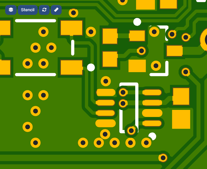
I’m currently working on a new PCB Layout, however when I uploaded it to Aisler every Pad which is connected to a Polygon is “bigger” / has less Soldermask around it:
The larger solder mask openings are a shortcoming of our soldermask opening adjustements as highlighted here: Soldermask Opening Adjustment
If you wish that we are processing your soldermask 1:1 as drawn, open up a feature reguest so the developers know that its a priotized feature. 👥 Feature Requests - AISLER Creative Community
Please also note that we do not check the soldermask layers in our PCB viewer, you thus have to ensure that your design complies with our design rules.