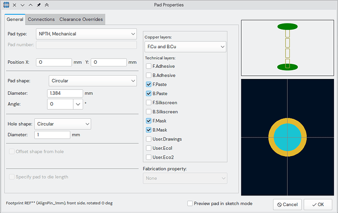
Afrer having to manually align the stencil in the initial revisions of by boards, I’m now looking at placing some alignment holes, which I could later use to put pins in order to align the stencil with the PCB.
I’ve looked through several topics on the internet related to this and how to design this in KiCad, but none of them provided a precise answer to my needs, especially that the end result may vary depending on PCB manufacturer.
I’m designing my board using KiCad. Based on what I have read in various forums I have prepared a custom footprint with a single NPTH pad. I have selected both Paste and Mask layers. The drill diameter is set to 1mm, while the pad diameter is set to 1.384mm to compensate aperture adjustment.
Would such a pad configuration be correct?
