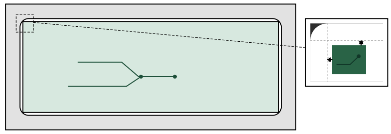
Designing electronics that combine a PCB with a 3D-printed enclosure often looks trivial in CAD. Everything lines up, the board fits perfectly, and connectors sit exactly where they should. In reality, this is rarely the case. Once real parts are assembled, PCBs may not sit flat, need force to fit, or end up under constant mechanical stress. The root cause is almost always the same: tolerances.
Different manufacturing realities
PCBs are produced with tight and very repeatable tolerances. Board outlines, hole positions, and thickness are well controlled.
3D-printed parts are different. Their final dimensions depend on the printer, material, slicer settings, and even print orientation. With common FDM printing, small deviations are normal and unavoidable. As a result, the enclosure is almost always less accurate than the PCB.
Understanding this difference is the first step toward reliable designs.
The PCB is the reference
A useful rule of thumb is to treat the PCB as the fixed reference and the enclosure as the adaptable part. A PCB should never be a press fit in a printed housing. It always needs some clearance.
Even a few tenths of a millimeter of space around the board can turn a difficult assembly into one that simply drops into place. While this extra space may look wrong in CAD, it reflects the reality of 3D printing.
Additionally, FDM-printed parts often produce slightly rounded or overbuilt internal corners, which can interfere with the sharp 90° corners of a PCB unless deliberate corner reliefs or added clearance are designed into the enclosure.
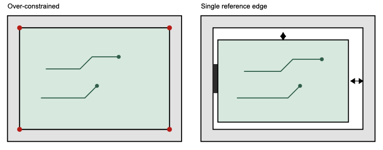
Positioning without stress
Clearance alone is not enough. How the PCB is positioned inside the enclosure matters just as much.
If the board is tightly constrained on all sides, tolerances stack up and the PCB has no way to settle naturally. A better approach is to define one clear reference, such as a single edge or stop. The remaining sides should allow some movement. This locates the PCB reliably without forcing it into a distorted shape.
Screws, standoffs, and mounting holes
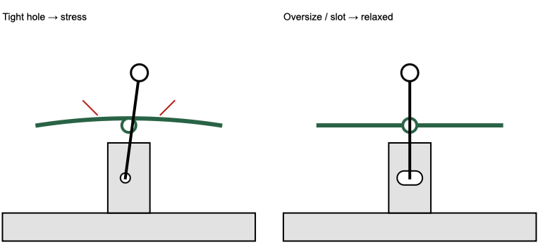
Mounting features are a common source of hidden stress. Holes in the PCB are precise, but printed standoffs are not.
If screw holes in the enclosure are too tight, tightening the screws can bend the PCB or introduce long-term stress. Slightly oversized holes or elongated slots in the housing allow the screws to pull the board down evenly, even if the print is imperfect.
Vertical tolerances matter
The Z direction is usually the least accurate in 3D printing. Problems often appear when a PCB is clamped tightly between the bottom of the enclosure and the lid.
Small height errors can cause pressure, bending, or rattling. Leaving a bit of vertical clearance avoids this. Flexible features such as snap hooks or spring-like supports can hold the PCB securely while still allowing small variations.
Openings for connectors and indicators
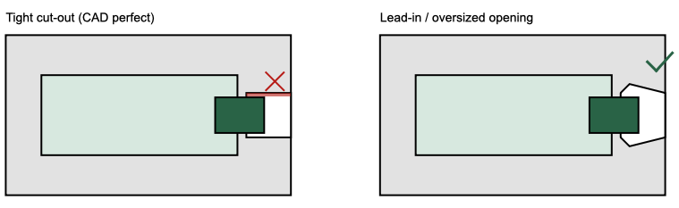
Connector cut-outs deserve special attention. A USB connector, LED, or button that lines up perfectly in CAD almost never lines up perfectly in the real print.
Slightly larger openings, chamfers, or lead-in shapes make assembly easier and often result in a cleaner final appearance. Trying to achieve a visually “perfect” fit usually leads to frustration during assembly.
What happens after assembly
Tolerance management does not stop once the PCB is mounted.
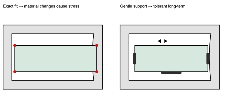
PCBs and 3D-printed plastics expand very differently with temperature. When electronics warm up, the PCB expands only slightly, while many printing materials expand much more. If the board is mounted rigidly, every heat cycle introduces mechanical stress.
This becomes especially relevant in sealed enclosures, LED projects, or devices that run continuously. A PCB that fits perfectly at room temperature may start pressing against the enclosure when warm. Allowing small gaps and avoiding rigid constraints gives both materials room to move.
Aging and environmental effects
Over time, additional effects come into play. Some 3D-printing materials absorb moisture or slowly deform under constant load. A design that relies on exact fits may feel solid at first but loosen or warp weeks or months later.
Designs that support the PCB gently, rather than locking it in place, are much more tolerant of these long-term changes.
Test early, adjust early
The safest approach is to test as early as possible. A quick prototype print or a simple dummy paper printed PCB can reveal issues long before final assembly.
Small adjustments made at this stage save a lot of time, reprints, and frustration later.
Final thoughts
Good tolerance management is not about being imprecise. It is about designing for real materials and real processes. When tolerances are handled well, PCBs fit easily, assemblies remain stress-free, and even simple 3D-printed enclosures feel robust and well engineered.