Hello,
We are Triton, a student association in Aachen. Our goal is to participate in the Microtransat Challenge, where the objective is to cross the Atlantic Ocean with a small, unmanned boat.
Our boat is about 2.4 m long and 0.75 m wide. On the 1.5 m² of usable deck surface we have installed solar panels, which will be our main energy source for the 6000–8000 km long journey. Since the sun doesn’t shine at night and cloudy days must also be bridged, our boat is equipped with two batteries.
The propulsion and steering are completely electric and are achieved via a thruster and a rudder, respectively. In addition, the boat carries all the necessary control and communication electronics.
However, 1.5 m² of solar area is not much. With a typical efficiency of about 20%, this results in a peak power of roughly 300 W. Furthermore, the sun only provides this level of power for a fraction of the day. As a result, we are operating under a rather tight energy budget. To manage the limited energy available to us, it is essential to monitor how much power is being generated and how much is being consumed.
This is where our Power Board comes into play. It acts as the central node of the entire power system and therefore represents the root of our wiring harness. On this board it is straightforward to place current sensors, Hall-effect sensors in our case, and collect all relevant data.
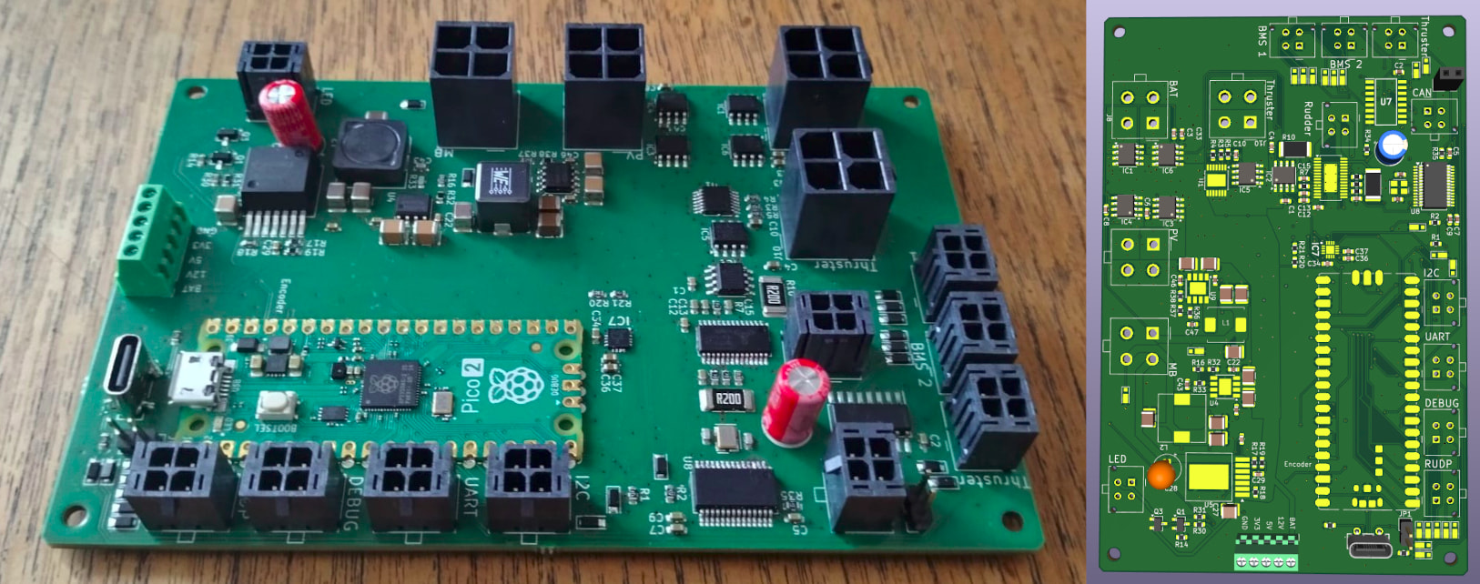
Another advantage of this central board is that it simplifies the implementation of on/off switches for individual subsystems. Ideally, devices should be switched off gracefully through software, but in some situations it is necessary to cut the power completely to limit potential damage.
Overall, our system operates at relatively low power levels, so the standard 35 µm copper thickness is more than sufficient. However, during certain maneuvers the propulsion system may suddenly require significantly more power. When looking at the resulting currents, one might start to worry about trace heating. To address this, we used the two inner PCB layers as ground and the two outer layers for V_dd in these critical sections. This works quite well: we were able to pass more than 30 A through these areas without active cooling and without significant heating of the PCB. The only thing to keep an eye on is the current rating of the connectors ![]()
We would like to thank Aisler for sponsoring our project and enabling both its realization and our continued learning and development.