Hello,
For this year’s AISLER Vrijmarkt challenge I decided to write about a project I have recently been working on: A custom Game Boy Advance cartridge that lets me turn my old childhood Game Boy Advance into a custom monitor that I can connect to my PC via HDMI. This would, for example, allow me to play emulated games on the PC or the Nintendo Switch virtual console directly on the screen they were designed for. It also makes it possible to play games or use any other software on the Game Boy Advance screen, although that has turned out to be less useful than I initially hoped, as most software does not really support the resolution of 240 by 160. It has been a very interesting project, requiring me to learn quite a lot about working with FPGAs to be able to complete it.
Let me start this by showing a photo of the finished project displaying my Windows background over HDMI:
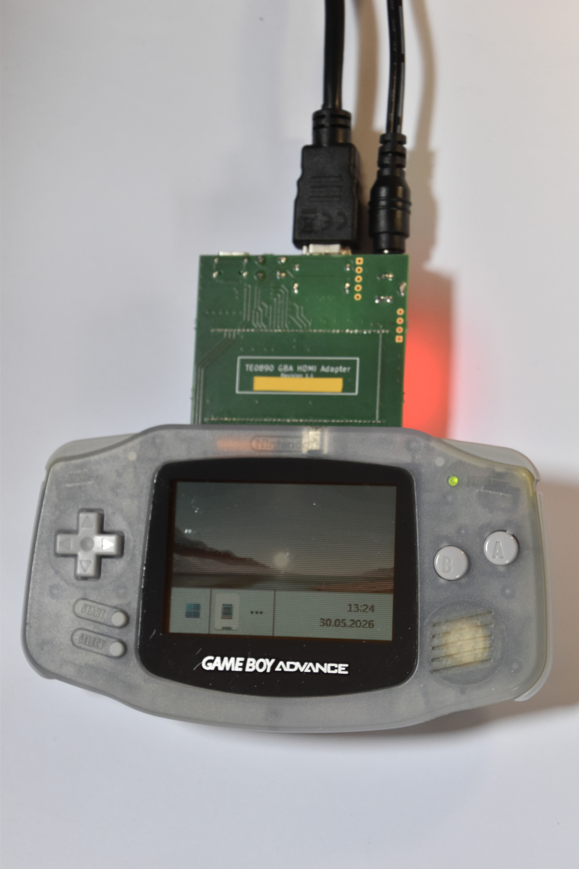
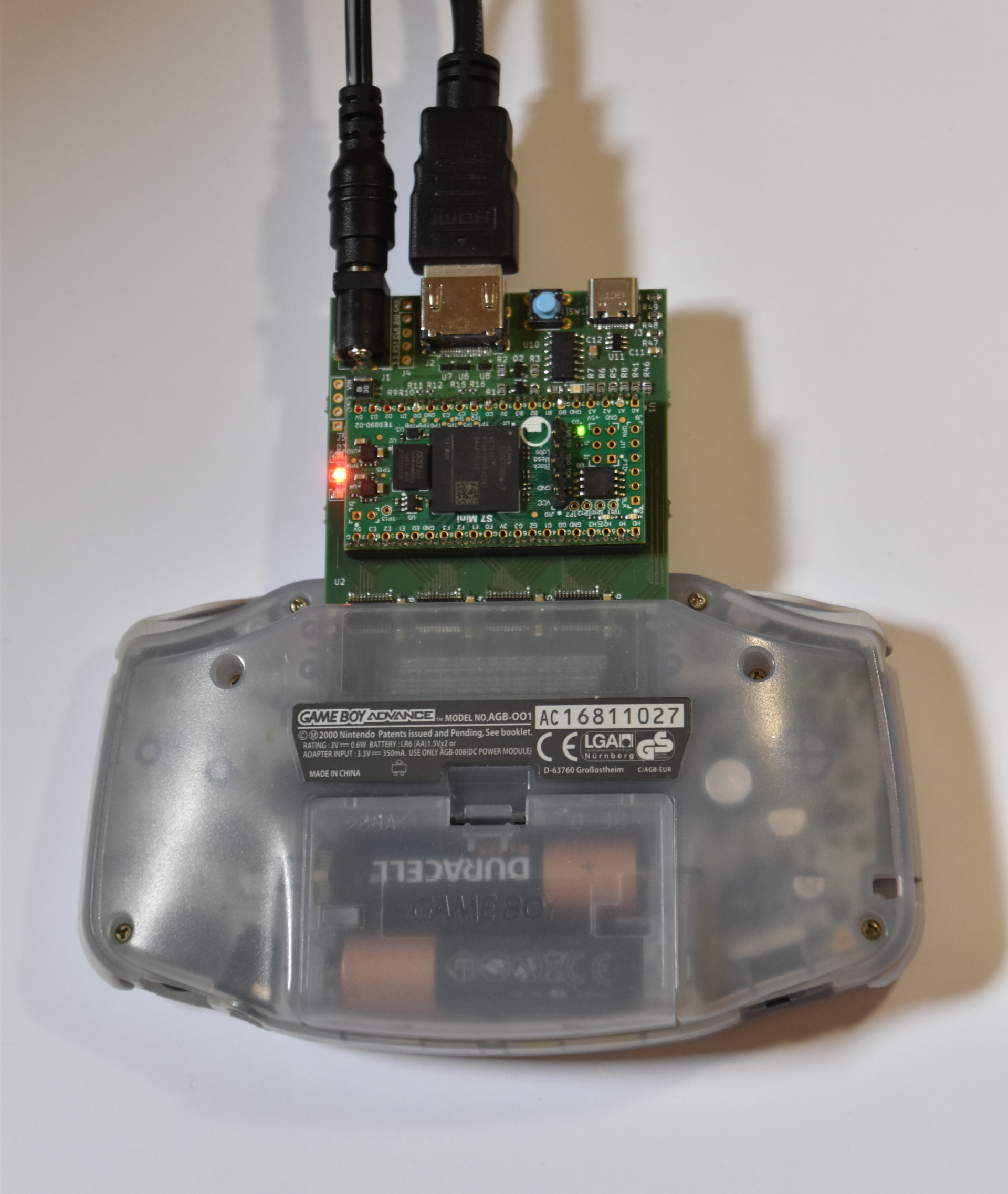
On this image you can see a Game Boy Advance that has a custom four layer PCB (designed in KiCad, manufactured by AISLER, assembled by hand) inserted into its cartridge slot. Two layers were not really an option because I needed controlled impedance differential pairs for HDMI. The tape is just there to censor my name which is printed onto the silkscreen. I decided to design the PCB in a way that made it fit the cartridge slot directly, without the need of a case because I do not really have access to a 3D printer to make a case and this was mostly intended to be a prototype. The Game Boy Advance itself is completely unmodified, so it can still play any games, and the custom PCB works on any Game Boy Advance, it should even work on a Nintendo DS.
It should also be obvious that both the resolution and the general quality of the display are not great. This is simply a limitation of the original Game Boy Advance, which has a resolution of 240x160, 5 bits per color and no backlight. This unfortunately makes taking high quality pictures quite difficult.
Now, since all components are on the other side of the PCB, let me show you a full picture of that side:
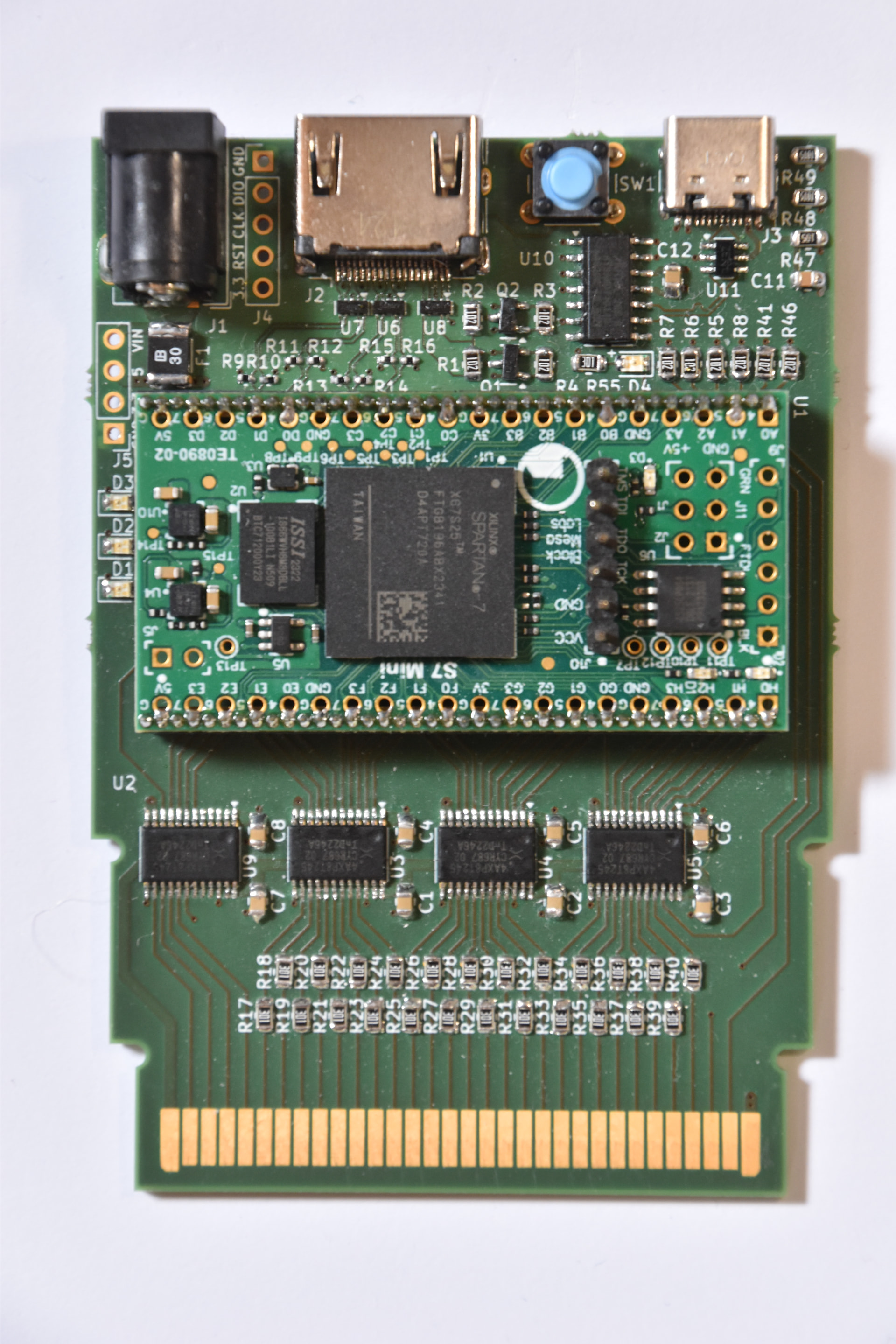
This PCB is built around the Trenz Electronic TE0890 FPGA module, with an HDMI input for the video data, a barrel jack for power because I was not sure how much power the FPGA design was gonna need when I designed the PCB, and the connection to the Game Boy Advance cartridge slot via level shifters which are there mostly for protection because the Game Boy Advance does also have a 5V based mode. There is also an USB C port that is connected to the FPGA via an ATSAMD11 microcontroller that handles the USB full speed communication for both audio input and HID (controller) output, but I have not actually implemented either of those features yet.
This is a simplified diagram of the connections on the PCB:
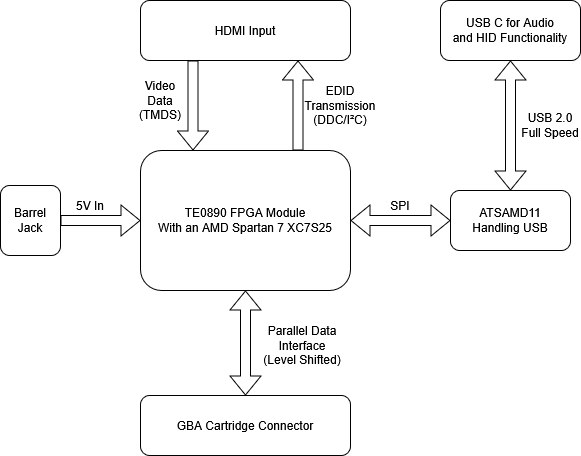
I chose to use an FPGA for this device because taking in data via HDMI while also sending data to the Game Boy Advance via the parallel data interface of the cartridge slot is not really something a microcontroller would be suitable for. The HDMI data coming in consists of three separate data streams with a bitrate of at least 250mb/s each, which is too much for a large majority of microcontrollers. The timing of the parallel connection is also completely controlled by the Game Boy Advance, which makes the time available to put the correct data for the current address on the bus relatively short. This by itself might be fine for faster microcontrollers, but both of these issues combined made an FPGA based device the correct choice in my mind. I might, however, also just be biased because I wanted to learn more about FPGAs, which, realistically, is the main reason this project exists in the first place. ![]()
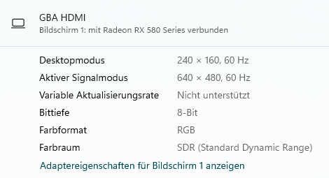
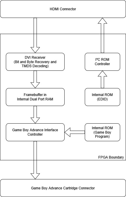
The HDMI part of the project was probably the most difficult for me. The hardware design was relatively simple, with the most critical part being four controlled impedance differential pairs that are terminated to 3.3v via 50 ohm resistors for the HDMI input. The FPGA development side of this was where I had to learn a lot, mostly because this was by far the most complicated FPGA based project I have worked on so far. I won’t go into too much detail, but in order for a PC to send any data over HDMI at all, it first needs to be able to read a data structure called EDID that describes the capabilities (resolution, refresh rate, color space etc.) of the monitor. This already took a while to get working, but it was honestly quite exciting to see a monitor called “GBA HDMI” in my PC’s settings for the first time. After that, once the PC starts sending video data in the format previously described in the EDID, there is still quite a bit of data processing to be done to turn that back into raw pixel values. I ended up implementing a DVI receiver from scratch using the DVI specification. HDMI is downwards compatible with DVI, which is quite a bit simpler at the cost of losing audio data via HDMI and a couple of other things.
At this point, I had the video data in an internal RAM buffer inside the FPGA. The next step was displaying that data on the Game Boy Advance screen. The way this works is by memory mapping the internal RAM buffer to a certain address range that the program running on the Game Boy Advance constantly reads from and writes to the internal video memory. This was a bit more complicated in practice, as the rate of data required to reach 60 frames per second on the screen is relatively close to the maximum bandwidth of the cartridge connector, so the copying of data has to be done using DMA, as the processor would be too slow. This is done by a custom program I wrote that is also stored on the FPGA and supplied via the cartridge slot. The GBATEK Game Boy Advance technical reference has been a huge help in understanding how the Game Boy Advance works.
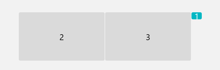
This is a diagram of roughly what is happening inside the FPGA:
Creating this project was definitely worth it from a learning point of view. From an actual usability point of view, the result is not great, it is too bulky and unwieldy, especially with the multiple cables, and the original Game Boy Advance’s screen is just not great. It is, however, still very interesting as a novelty item.
This was intended to be a prototype and I still might make a second version of this with power, video and data over a single USB C port, while also trying to fit it into an original cartridge. This would require me to work directly with the BGA FPGAs instead of a module like I currently do, which is probably not really feasible for me right now.
Full disclosure for the purposes of this challenge: I had already been working on this project for quite some time before the announcement of the AISLER Vrijmarkt challenge, so this is mostly a writeup about a pre-existing project. I personally do consider this a “reuse” project and think that it does fit the spirit of this challenge, but that is not for me to decide.
Thank you for reading.
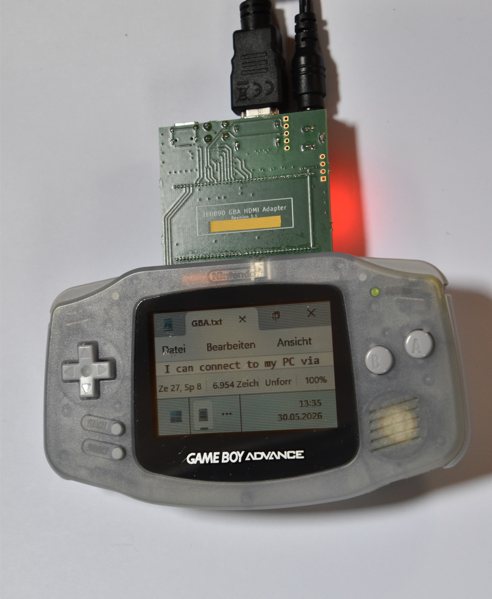
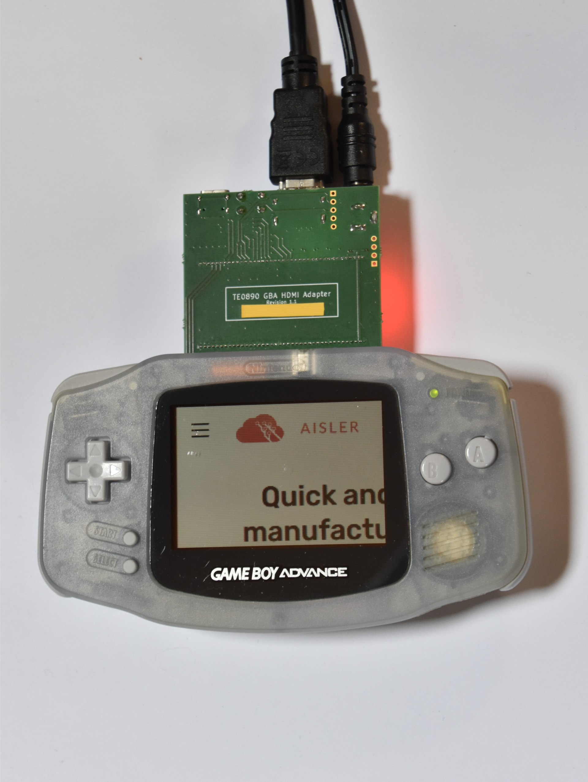
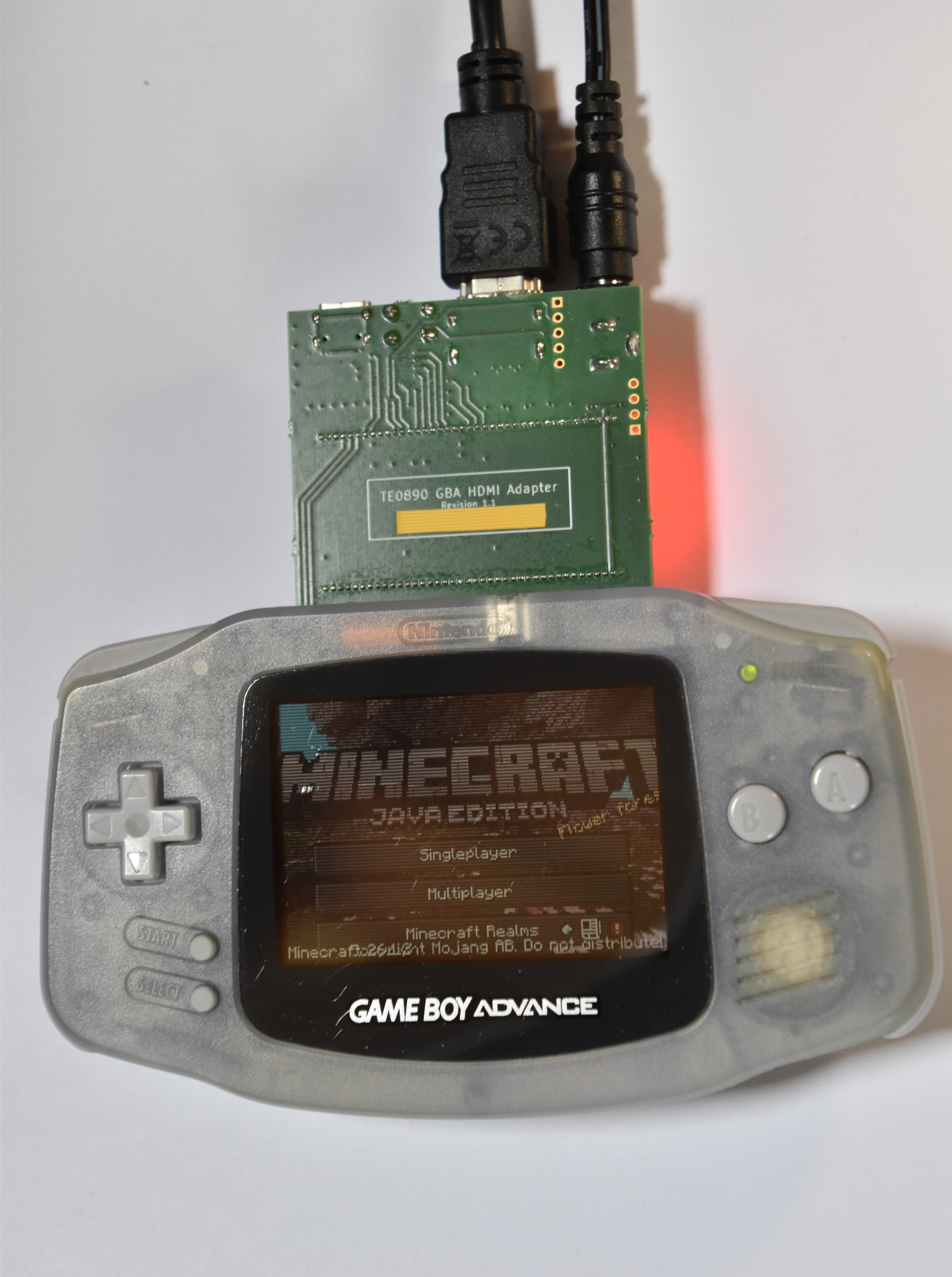
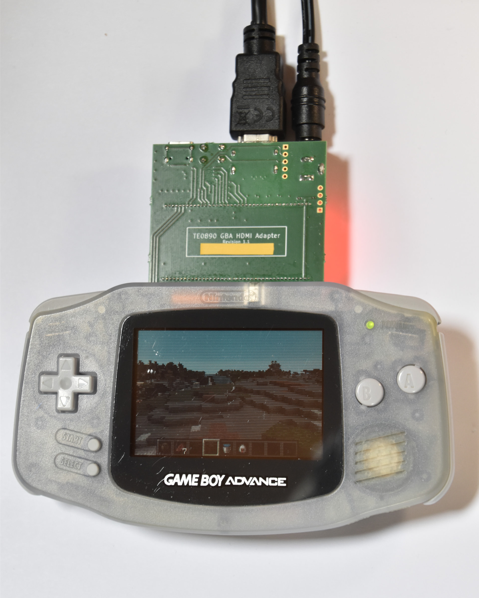
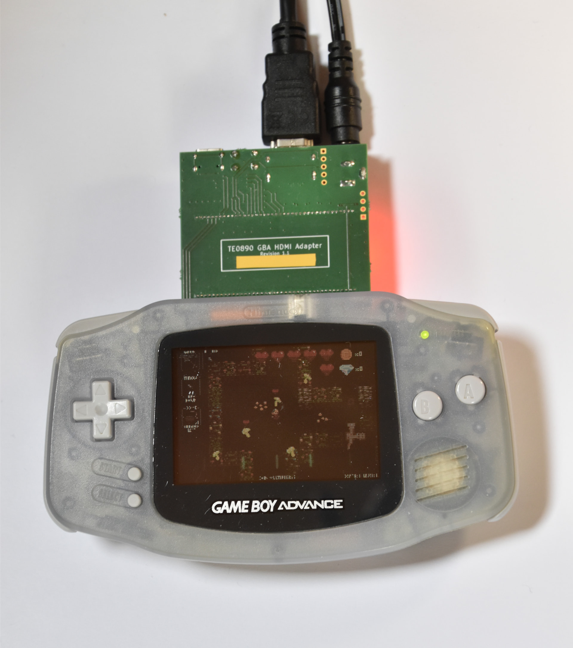
Lastly, here are a couple more pictures of the monitor showing various applications and games: