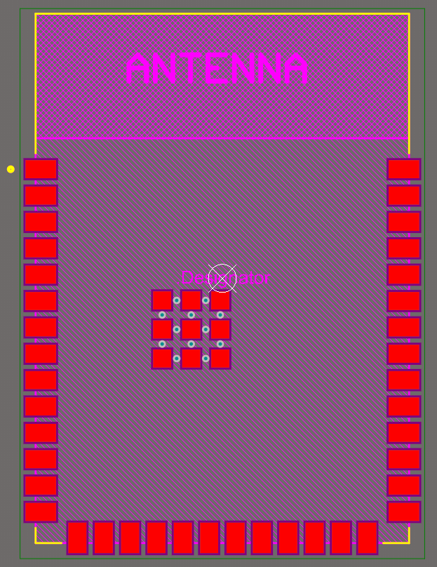
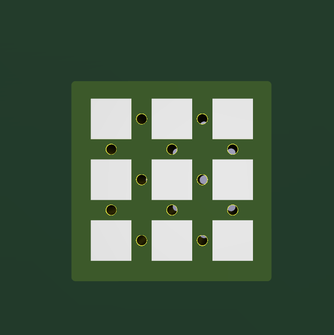
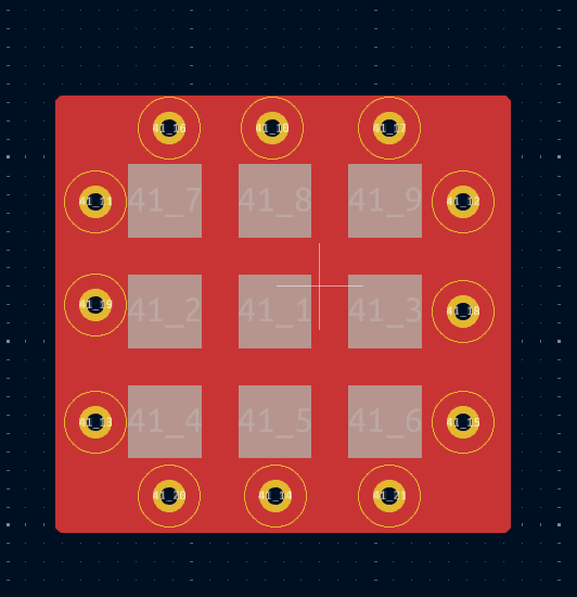
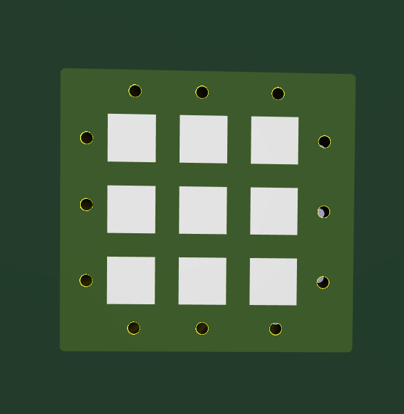
The problem is that in the center of the components there are some GND pads and vias (0.2mm hole & 0.4 total diameter) that seem to be smaller than manufacturing capabilities.
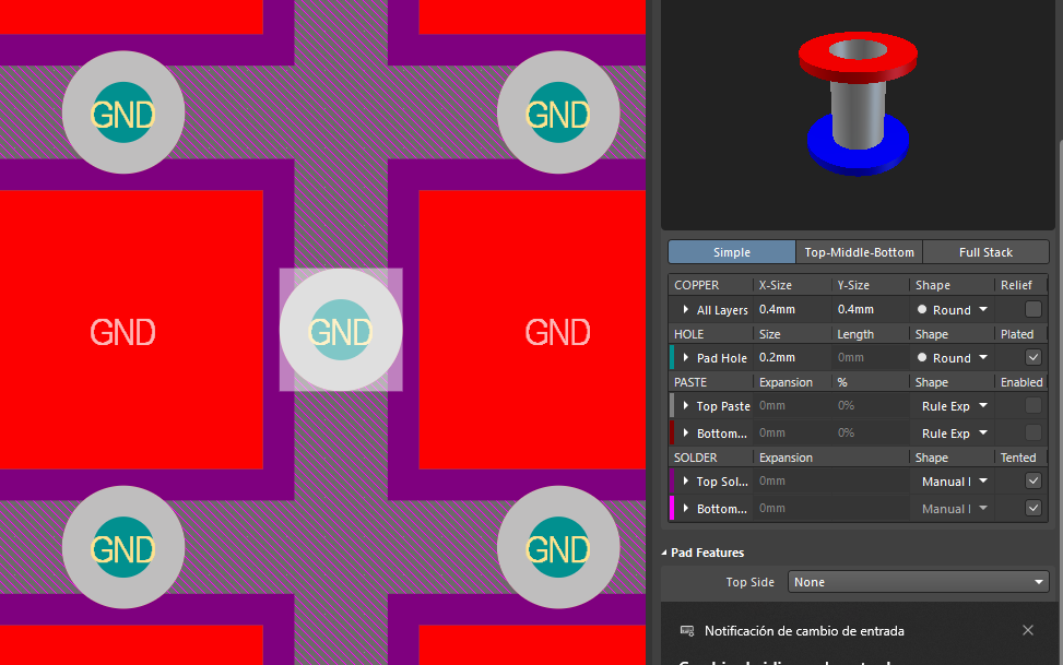
Please note that the soldermask expansion set by SnapEDA is unnecessarily large, I’d set that value to something more reasonable or keep it at 0 µm.
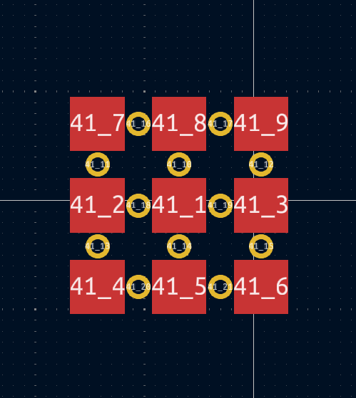
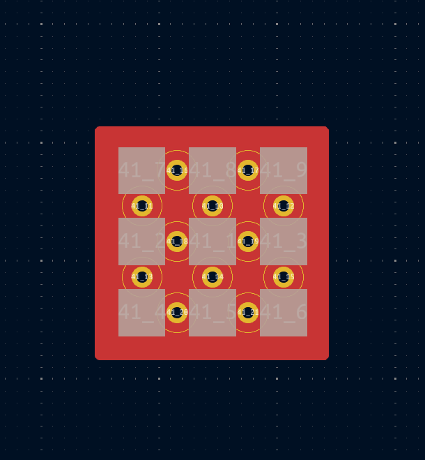
Another approach I would recommend is to place the vias around the pads, this ensures that no soldermask can wick into the vias. By doing so, you can also use a larger via diameter and potentially even our budget option.