With the new 0.1mm resulting via drill size for complex 6L boards, I just might be able to use your services for boards with somewhat finer BGA footprints. I have a BGA with a 0.65mm pitch and 0.33mm pads. To fit a via squarely between pads of the BGA, with a 0.125mm spacing to the pads, I would need to use a 0.33mm wide via. I calculated that you currently support sizes down to 0.5mm. Also, I saw that you do not support via-in-pad.
It would be great if you guys can confirm my calculations/assumptions above. Also, my question is this - will your fab houses build the boards if I violate their capabilities, slightly? I would be willing to take the risk for a prototype board, if I knew what is more risky (the final via size, or the spacing around the via) and how risky it would be (as in “don’t even try”). For example, how risky would it be with 0.4mm vias with a 0.1mm clearance.
You can still order the PCBs if they do not comply with the design rules. But you waive our manufacturing guarantee and will not get a refund or free remanufacturing if the design doesn’t work out.
0.4 mm vias and 0.1 mm clearance is the “safer” approach. You will also need an even copper distribution for equal plating across the board.
This is a timely question as I am also considering using 0.4mm vias with 0.1mm hole. This results in an annular ring size of 0.15mm, which is 0.05mm under the 0.2mm annular ring specified in the design capabilities. It sounds like there is some risk with this though.
So is a 0.5mm diameter (0.1mm hole), the smallest via that compiles with the latest design rules?
As stated in our DRC 0.5mm diameter with 0.1mm drill is the smallest Vias we do. I interpreted your question as " If I violate DRC what would be the safest way to do it?"
For context, I’m now working on a board that makes use of the 0.1mm drill, and it is already proving useful for accommodating newer components; however the 0.2mm annular ring requirement is now a limiting factor.
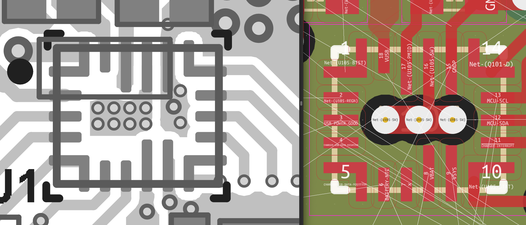
For example, this is a layout for the Texas Instruments BQ25620 that I am working on today, with three central 0.5mm vias. TI’s evaluation reference board shown in gray beside it…