Hi, I’d like to use an FUSB302BUCX, a WLCSP-9 package that’s probably designed for HDI. there’s only one pad that’d be problematic, namely the center B2 interrupt pad. At the risk of broken boards, though, a 0.5mm via just about fits but would violate spacing.
I am curious what the failure rate would be (and I’m fine with vias draining solder and waiving any warranties) if that were to be etched. JLCPCB can do it with via in pad or with their much smaller via/drills.
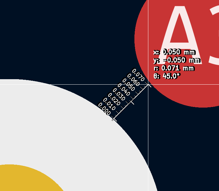
With a 0.2 mm drill (compensated 0.1 mm) and 0.125 mm annular ring, you’ll get roughly a 0.45 mm via. This gives you a clearance of ~70 µm ~44% smaller than what we support as the smallest size. I tested 100 µm with ok yield a while ago. But that requires a good copper balance.
I cannot make a statement about 70 µm clearance.
Furthermore, you will basically have a very poor connection as the solder balls are basically the same size as the drill.
I highly recommend the WQFN14 of the FUSB302B which we can manufacture with no issue.
Other manufacture may offer you features for smaller runs for free, but they add substantial cost on larger production runs. So if your design requirements allow it it makes sense to choose a traditional manufacturing process and choose the package accordingly.