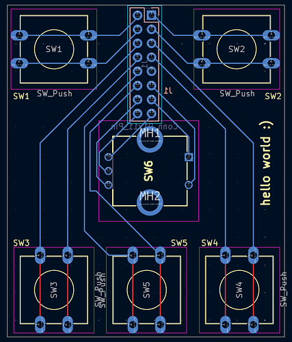
Hello! I’m trying to design and manufacture a PCB for the first time. I want to have 5 buttons and a rotary encoder on the “front” of the PCB and a 16 pin header on the bottom. I have designed this PCB for it but I have absolutely no clue if it works or not as I’ve never done this before. Any help or advice would be greatly appreciated. Thank you
Hello! I’m trying to design and manufacture a PCB for the first time. I want to have 5 buttons and a rotary encoder on the “front” of the PCB and a 16 pin header on the bottom. I have designed this PCB for it but I have absolutely no clue if it works or not as I’ve never done this before. Any help or advice would be greatly appreciated. Thank you
Will it work? Probably.
- The wires look quite thin, what thickness are you using?
- Double check the holes are the right diameter for your pins and buttons. I got a bad footprint once, the holes were smaller than the pins, and had to attach it floating.
- On the left side you have two wires going pretty close to each other. I don’t know if that is below the limit, but there is no reason to push it, you have plenty of space.
- You have two layers, why not use both for routing? The pin header is through hole, so it can connect on both the front and back. That way you can make SW5 and 6 neater, although the traces would be visible at the front (if you care about that).
- You should add a versioning on the silkscreen, so once you make revisions you know this is v1.
- I don’t know how your circuit is set up, if you just want to detect a button press, one end of the button goes to a pull up resistor and an input pin in the MCU, and the other to ground. This means all the buttons can use a common ground, which would get rid of four pins in your header. But maybe it makes sense in your case.
The suggestions by @Davidmh cover many great points! I second the opinion on the trace thickness. You also have plenty of space on your PCB, so I would add debouncing circuits for the button on the PCB too. If all parts share the same ground, it would also help with the manufacturing if you use a ground plane on top and bottom and stitch them with vias. That makes manufacturing easier for us too ![]()
Würth Elektronik provides a guide on how one can debounce buttons here: https://www.we-online.com/catalog/media/o185480v410%20SN015_Contact%20debounce%20circuit%20for%20switches.pdf
You can find their buttons and rotary encoder here: Switches | Electromechanical Components | Würth Elektronik Product Catalog
Okay first of all thank you guys so much for the advice!
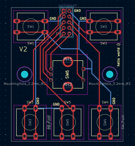
A bit after uploading the first post and after reading your guys suggestions I designed this:
Putting them all on a common ground definitely helped, along with using the different layers. I read through the guide about debouncing buttons and it definetly seems helpful so I will have to look into that as even stuff like that feels very complicated to me.
After I researched a bit it seems like a ground plane is simply a patch of copper that all GND nets connect to that then goes to ground, is that correct?
I have also adjusted the track width to be 0.4 mm, seeing as these won’t be carrying lots of current at all I think this should be fine? Again, never done this before so I’m not really sure.
Thank you so much, both of you for helping ![]()
The GND label on the upper left seems wrong, the other leg is the one connected to ground.
By the way, good on the mounting holes. It makes it much easier to assemble in practice.
After I researched a bit it seems like a ground plane is simply a patch of copper that all GND nets connect to that then goes to ground, is that correct?
Yes. The main advantage is that you’d have a very low impedance return to ground, which is important in high speed or analogue signals. In this case, it most likely doesn’t make a big impact, but it is good practice anyway.
Since you only care about high or low values, and you probably have a lot of margin, your grounding is fine. But if you want to learn more, this is a good application note: Staying Well Grounded | Analog Devices It explains why you should use a star ground topology, and the most common pitfalls. But this is just for gilding the lily.
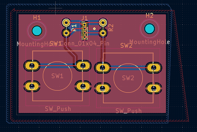
Here is how it would look like with a ground plane:
Don’t look too close at the rest, it was a quick and dirty example. But I did put a via between R2 and J1 so that area is filled too.
A ground or any copper plane also makes manufacturing easier during the plating stage.


