Introduction
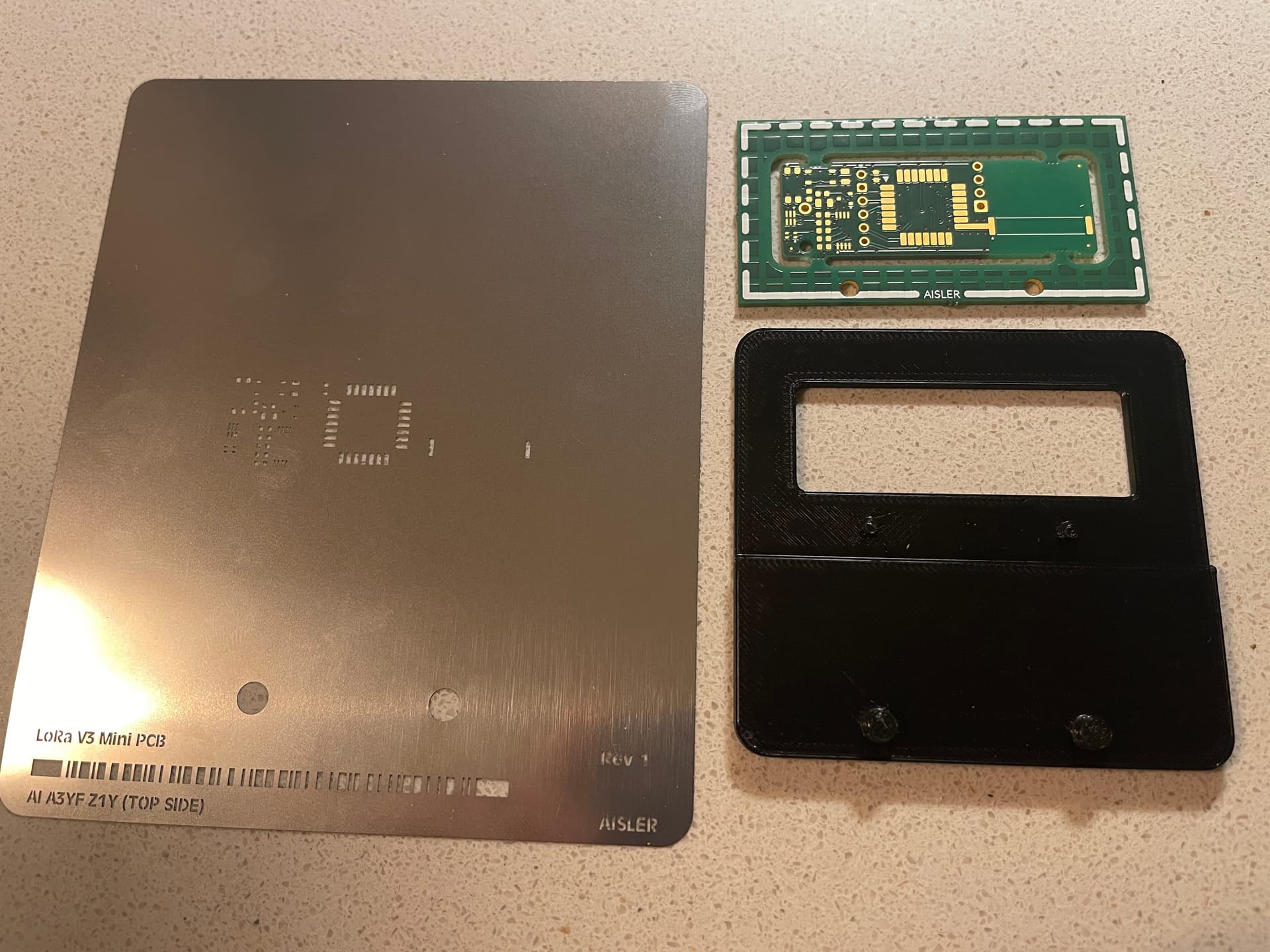
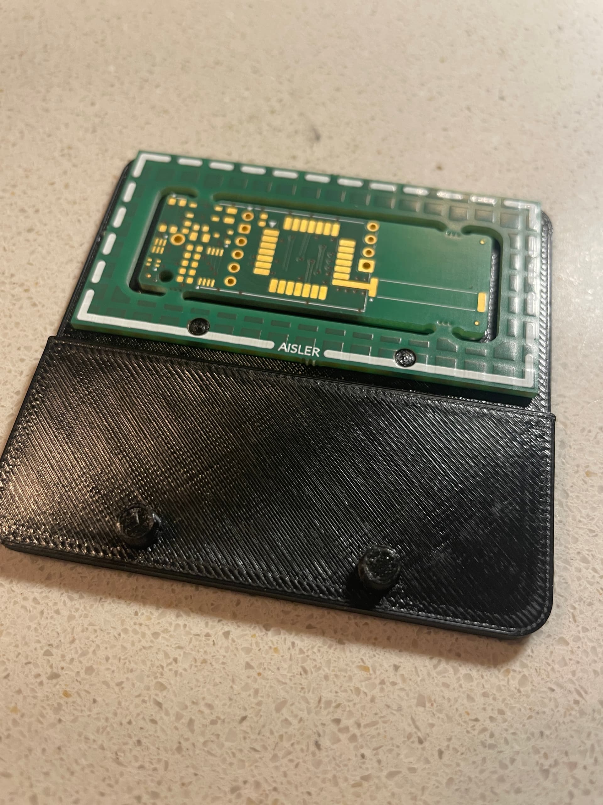
When prototyping PCBs with SMT components, you need to apply solder paste. Aisler can provide you with a matching stainless steel stencil, aka the Stellar Stencil, which is of great help.
Still, aligning the PCB and the stencil is not always easy, as component pads and pitch gets smaller and smaller…
EuroCircuits and Aisler are offering the so called ‘stencil registration’ : when selecting this option, the PCB and the Stencil will each have a pair of holes, which allows to align them with a certain tool. The official alignment tool comes in two versions : a more professional one which is about 1500 euro, and a more affordable hobbyist version.
But if you have access to 3d Printing, it is very easy to 3DPrint this tool yourself.
Parametric
In the Stencil Registration standard, the holes are set apart with a distance which varies according to the size of the PCB. So its not possible to have one tool for all possible PCBs. But with this FreeCAD model, it’s still very simple : the model is ‘parametric’ which means it has some parameters which you can enter, and the model will adapt to them. In this case, eg. enter the dimensions of your PCB and the model will adapt itself to a stencil registration tool of the correct dimensions.
The FreeCAD model can be found here : github.com/Strooom/PCB-Stencil-Registration-Tool
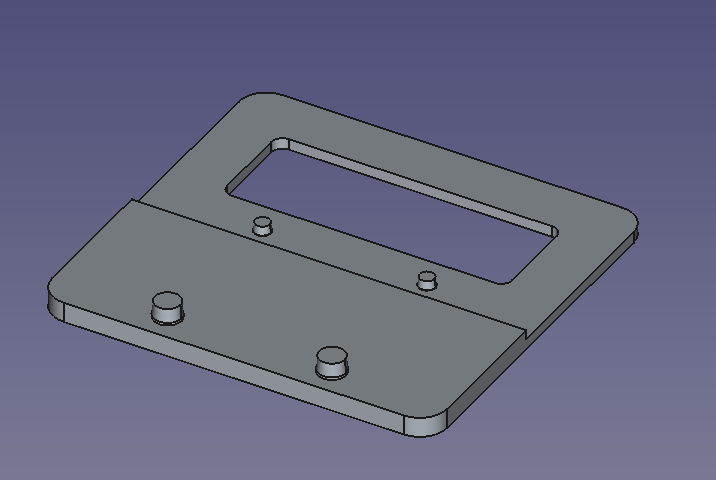
Example 1 : registration tool for a 52 x 18 mm PCB

Example 2 : registration tool for a 80 x 60 mm PCB
Parameters PCB Width, PCB Height and PCB Thickness are self-explaining.
There are more parameters to control the shape, they are all found in a spreadsheet ‘Data‘ found inside the FreeCAD model. If you open the model in FreeCAD, then open the ‘Data’ spreadsheet in the model, then choose menu ‘Windows | Tile’ you will see both parameters and model and it becomes easy to experiment.
When ready, you can export the model, eg as .step file (select the body and choose menu ‘File | Export…‘), load it into your favorite slicer and start printing.
Tuning for perfect alignment
The purpose of this tool is perfect alignment. To achieve this, you need a perfect fit of the centers on the tool and the holes in the PCB and stencil. 3D printing will always have some tolerances, depending on printer type, filament and the position of the moon, but don’t worry, the model is able to deal with that :
- a parameter ‘printMargin‘ has a value for tuning the diameter of the holes, starting from their standard size of 3 and 5 mm. When printed, the diameter will typically be slightly smaller than those values, so you can compensate by setting a positive printMargin of eg 0.1 mm to achieve a perfect fit. This will require a bit of experimenting on you 3D printer, but only once. Then for successive PCBs, you should be able to print the tool ‘first-time-right‘
- the centers have also a small ‘chamfer’ which means they are a bit smaller to the top and wider at the base. This conical shape helps in achieving a perfect fit when you press the PCB and stencil down on it. Again it’s a parameter, 0,2 mm works fine for me.
Single or Double sided
PCBs can have components on one side or both sides. With components on both sides, you also need solder paste on both sides, and you will get two stencils. When setting the parameter ‘singleSided’ to 0, you activate doubleSided PCB and an additional pocket is created so you can apply solder paste, flip the PCB and apply solderpaste to the other side. The tool can also be used during placement of the components. The ‘baseThickness’ parameter is set to 2 mm by default, so when your components are higher than that, you need to increase this value.

More info about Rapid Registration
Rapid Registration - ![]() Knowledge Base /
Knowledge Base / ![]() Services and Capabilities - AISLER Creative Community
Services and Capabilities - AISLER Creative Community