Good day, im porting some settings about the specs of the 4 layer stack up in altium, need more info coz i must calculate an impendance for an RF strip line.
Suggestions and corrections are well appreciated
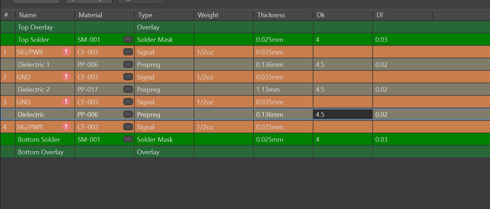
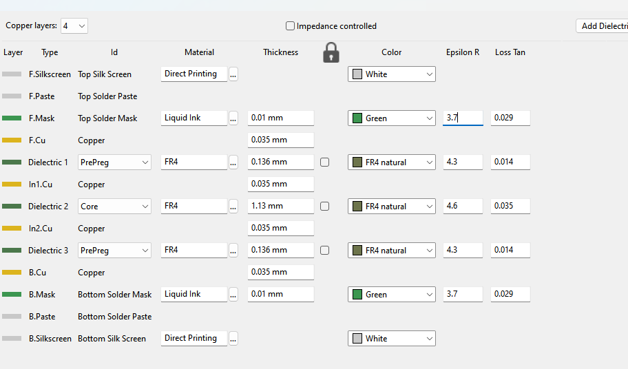
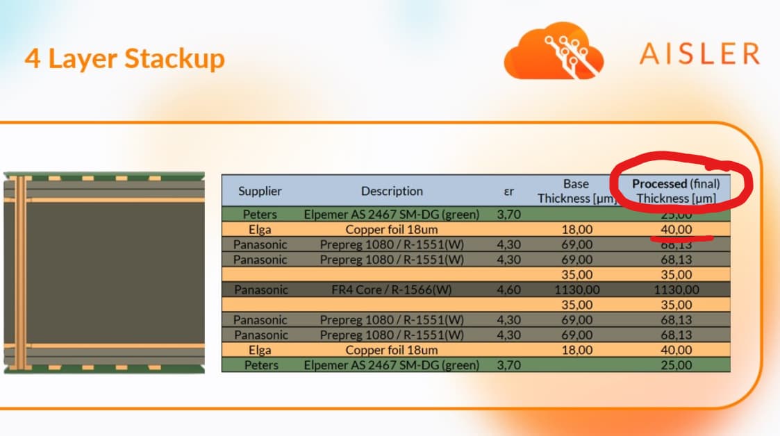
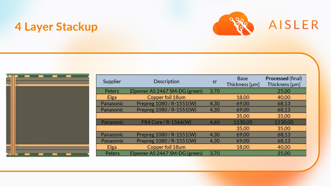
The layer thickness and copper weight are not correct yet, the Er value also needs to be adjusted. We have these documented in our 4 Layer article. Please note that you need to use the final dimensions.
thank you for your info… the size refered in millimeters can be ported also for altium stackup setup?
Waiting for a kind response
Regards
David
How do you mean this? You can enter the values in Altium the copper thickness is 0.035mm → 35µm → 1 OZ
okay thank you for your informations… i will check it later
please send me link for Altium 4 layer stackup
Good day, I’ve found in this rep some info about aisler
it’s only published the altium 6 layers stsckup… miss the 4 layer stackup and i don’t remember well if aisler pcb stackup parameters are correct
Hi Thea,
This differs from your post https://community.aisler.net/uploads/default/original/1X/7697769deec9bcacbd18ab5e83a5315bcc8ab70b.jpeg
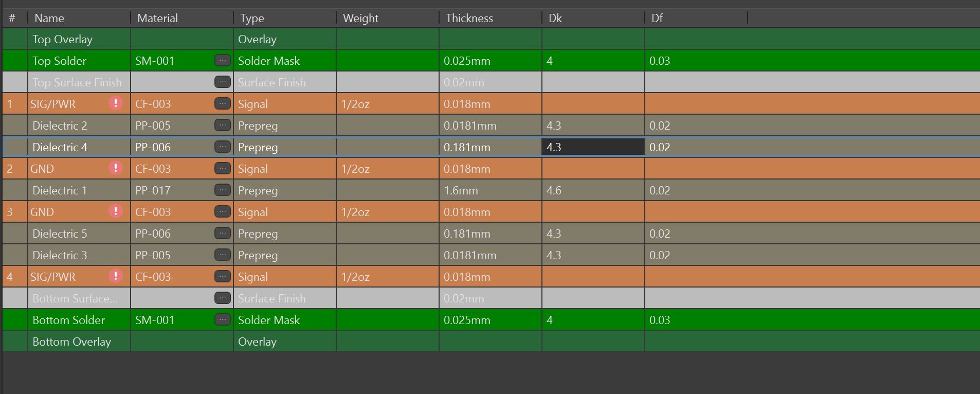
F.Cu and B.Cu 0.035 != 0.018
Which is right now?
Hi,
As mentioned above, the Github templates say the outer copper layers are 35um thick, but the stackup diagram says 18um.
I’m assuming the template is just a typo and the stackup is actually 18um thick on the outer layers?
Thanks