First things first, we prepare your design files for manufacturing using an automated software pipeline, if you have any questions or want to make remarks, please contact our support before ordering, as we do not read notes included in your project files.
Open up your PCB file and make sure all planes and polygons are updated, make sure to run the DRC to catch any errors, if there are any, please resolve them.
If that is done, navigate to Output → ODB++
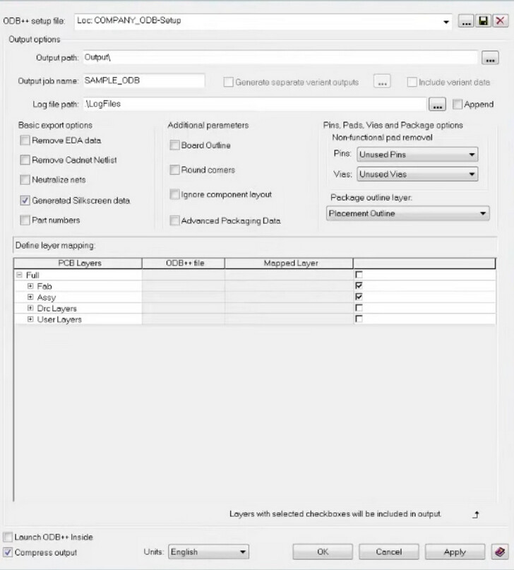
This will open a window with multiple options.
Make sure to include the required Fabrications (Fab) and Assembly (Assy) layers. If you use a custom layer like aisler-bridges, include it in the User Layers section.
Do Not check Remove EDA data, Remove Cadnet Netlist or Ignore component layout, selecting these options removes data that is required for assembly and e-testing of the PCBs.
You can use Neutralize nets to replace your net names with generic ones, but we don’t recommend it because it makes it harder to compare the e-test report with your layout.
Tick the Compress Output checkbox so you don’t have to manually compress the files before uploading.
When everything is set up, press OK and save the .tgz file. The file will usually be saved in your project directory or in the location specified in your output configuration.
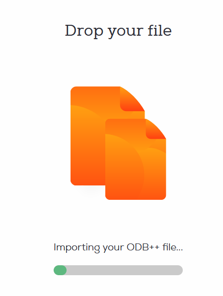
Now upload the file to our website, we will automatically generate the production data from it.
After we processed the ODB++ file you can inspect the boards using our board viewer.
We give a rendering guarantee that the boards are manufactured as displayed in our viewer. You can read this article if you are unsure how to use our board viewer or if you want to know how the rendering guarantee works.