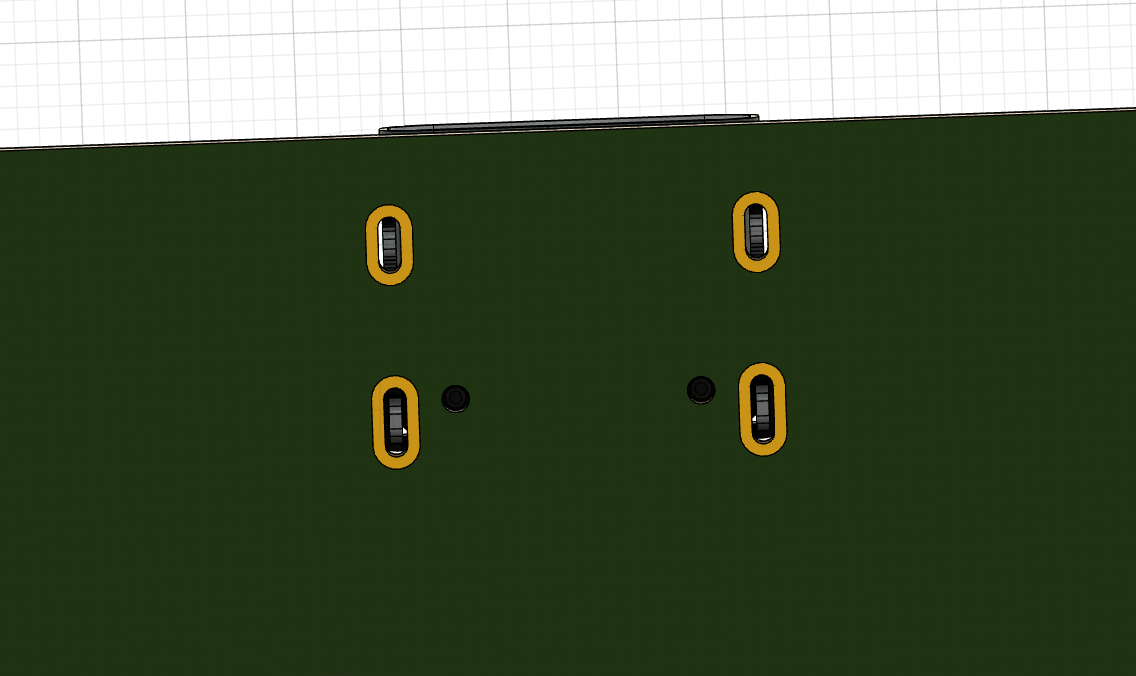
I’m designing a PCB in Fusion 360 and using a Würth USB-C port (629722000214). However, I’m struggling to correctly implement the plated slots (elongated holes) for the mounting pads, as the milling layer is not being processed properly.
Despite trying to follow the guide (I couldnt get it done like it was described there) and spending many hours trying different Gerber exports and footprint adjustments, I haven’t been able to get it right. The result is always holes that are too small instead of proper milled slots. I also reached out to Würth Electronics, but they haven’t been able to help so far.
Could someone assist me with this issue? If anyone has already successfully created a footprint for this connector, I’d be incredibly grateful if you could share it. I’m also happy to jump on a Zoom or Teams call if that helps!
Thanks in advance for any support!
Best regards,
Alexander
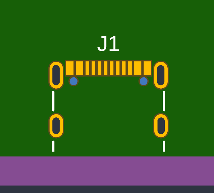
The guide was written by me a while ago, I will check if the steps still work. In the example I used the 629722000214 too, maybe I still have the file lying around.
I will come back to you asap.
Btw, we highly recommend exporting ODB++ files from Fusion as they include the BOM and Netlist so we can do E-Testing and Assembly.
Hey Thea! Thanks for the quick answer and your help. When trying to export as ODB I couldnt add the milling layer (46) cause it only allowed me to add layer 1-16. I’m sure there is a way but I am not used that much to fusion and pcb in general
When dealing with your tutorial I just couldnt manage to find the menu where you Disconnect symbol and footprint, so I didnt made it further. Also the unlinking of the library was a little bit different for me but I somehow atleast managed to just generate a copy of that usb-c port which I tried to modifiy.
The milling layers are not exported through ODB++ anymore as far as I am aware. That is why we need to change the footprint to use the plated slots.
Another method would be to import the EAGLE library and adjust the footprint there, that avoids the mess that is the" library.io" and “Autodesk Hub” integrations. (I very much dislike the forced cloud stuff )
Hi I managed to finally the menu where the footprint of the usb-c port is connected to the schematics, afterwards I was able to do just like in the tutorial mentioned and everthing is looking fine