Hi,
since Kicad now supports to remove inner annular rings from vias, I’d like to know if this is actually supported by Aisler or are the inner rings required by the production process for multilayer pcbs?
Cheers
Andre
5 Likes
I am also curious about this.
@Thea, hope you don’t mind the mention. Perhaps this can be included in the design rule update?
I will ask the production engineer and include it in the new DRC asap.
1 Like
Hi all,
This topic is also very interesting to me. I’ve exchanged a few emails with Thomas about vias and was about to send another about just this thing. I’m guessing that Ondre, like me, is asking about this because he is trying to route out a BGA.
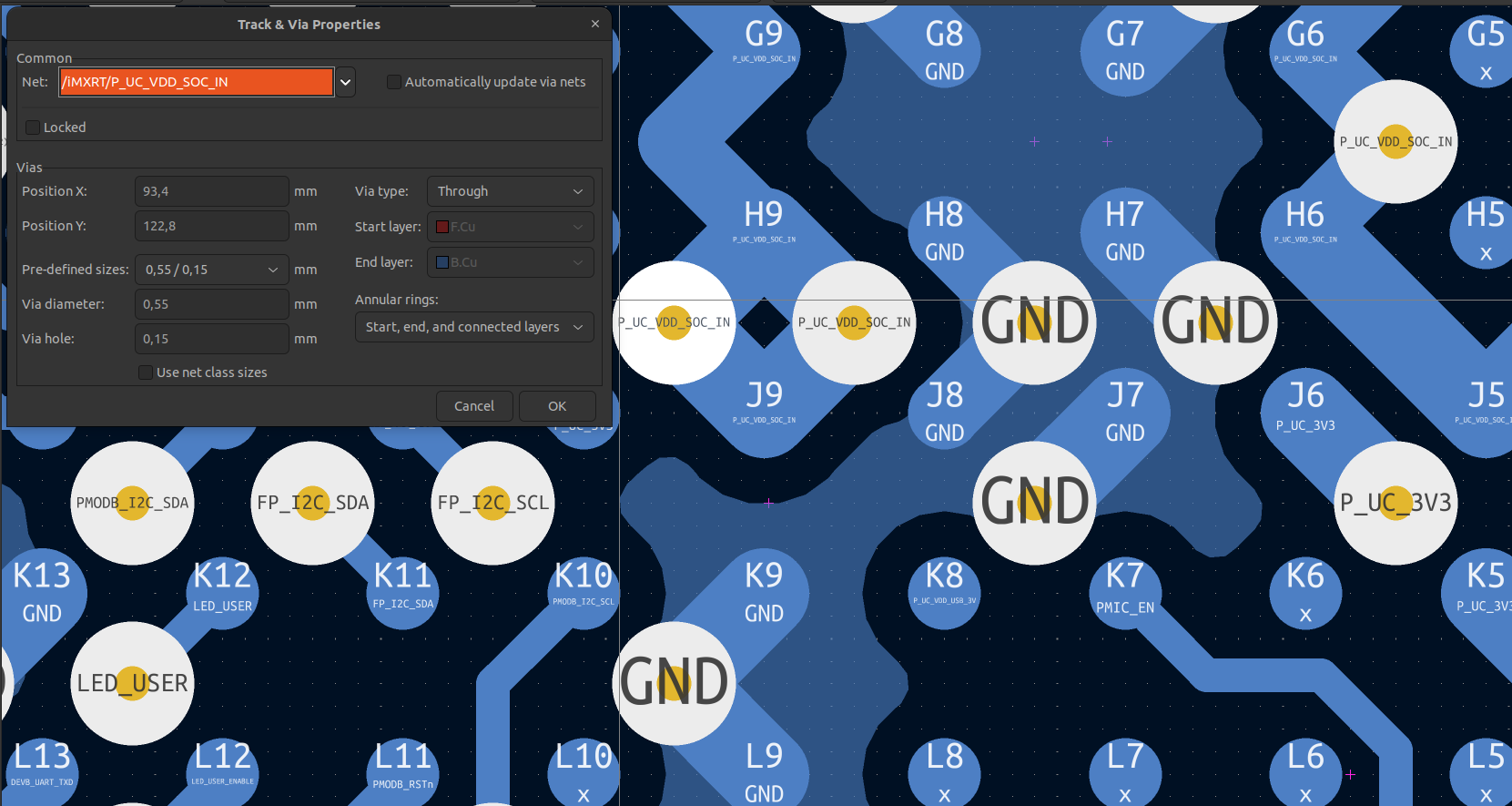
In my case, it is a BGA with a 0.8mm ball pitch and (really pushing the limit) 0.32mm minimum pad size. According to the Aisler rules for 4L, the smallest via we can use is 0.5 mm with a 0.1mm (I’m assuming that’s actually the initial drill size and that the via ends up getting almost plated shut)–I’m actually trying to use 0.55mm pads with 0.15mm drills because 0.1mm seems very small to me. I understand that due to the way Aisler builds boards, the 0.2mm annular ring minimum is a hard limit, but it is really quite large compared to more traditional PCB fabricators. No problem, I understand that it is the price to pay for the unique combination of speed and price Aisler achieves by batching the boards and using high levels of automation.
Changing the routing somewhat, I can probably work around the limitations of the 0.5/0.1 via for signals in my 0.8 grid, but there is another problem–the internal power and ground planes are left with huge gaps which are terrible for power integrity. I understand that the large annular ring spec is to ensure that vias are reliably connecting signals from one layer to another, despite some mis-registration between layers and drills. In the case of signals passing through inner layers, however, I don’t care if they contact the pad, in fact, I want them to NOT contact anything on that layer.
If the answer to Ondre’s question is that unconnected inner annular rings CAN be removed from vias, this addresses my concerns as well, and I would be very happy to hear about it. I also agree that this information, if true, would be another great addition to the already excellent online documentation.
Thanks,
-Kevin
I’ll create a render of what this topic is about.
Pictured: a 4-layer board with two vias where the former has a track on layer two and four, and the latter has a track on layer one and three. When each via would have an annular ring, this would not be possible.
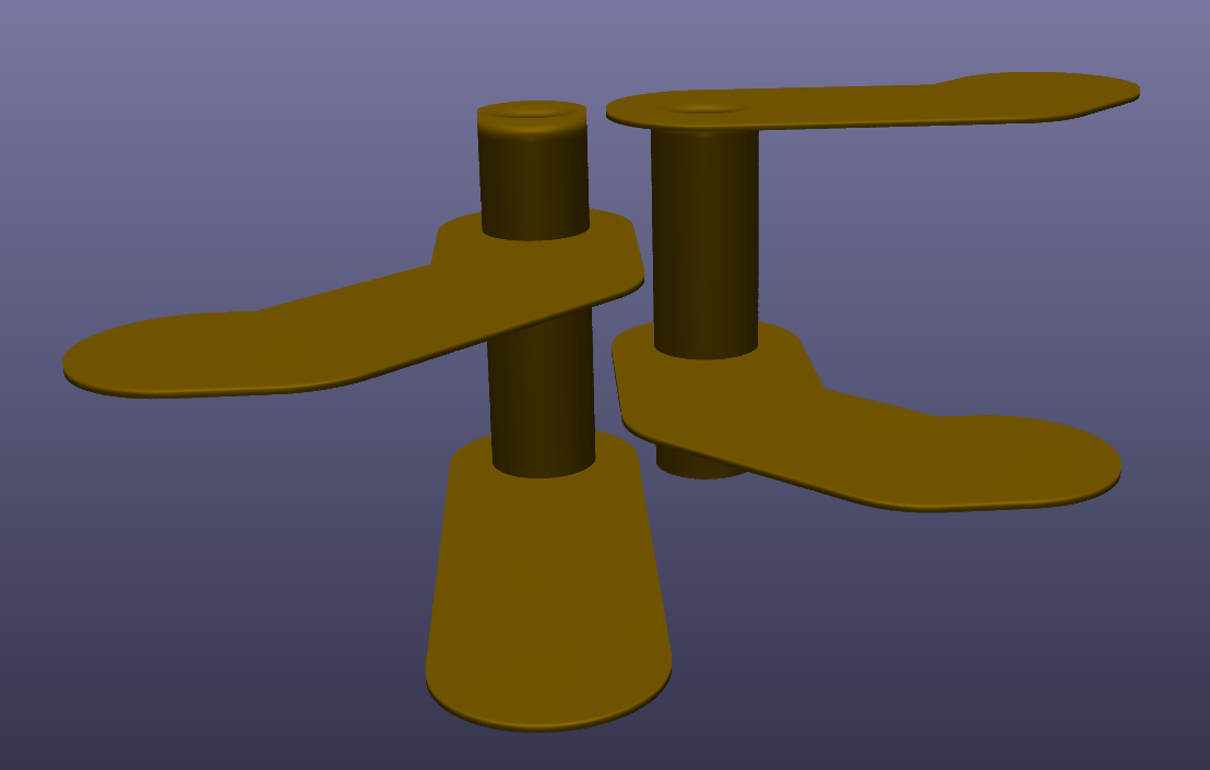
If each layer had an annular ring, this would occur:
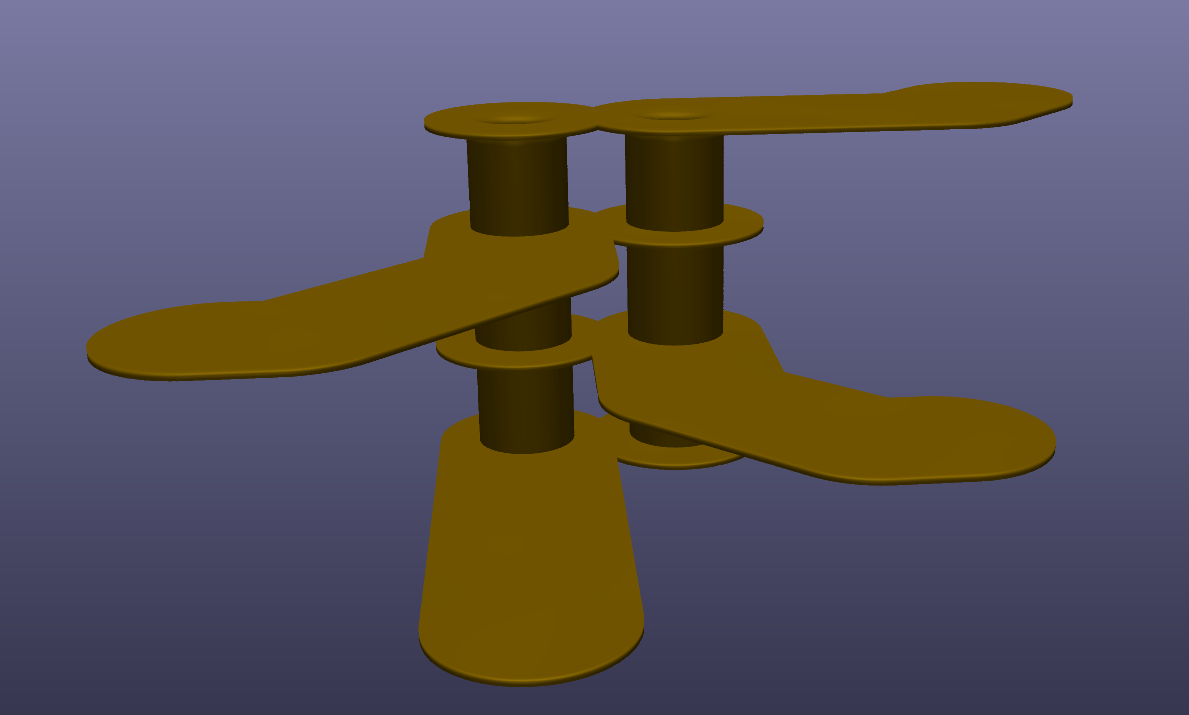
Images under CC0, feel free to use them in the documentation or any other use.
I can already say that the top image would not work. We require annular rings on top and bottom.
Hi again. I just wanted to mention that this issue and
2872 are intimately related.
Hi everybody. Just a friendly nudge to the Aisler team… I’m waiting to know if the inner unconnected rings can be removed or not to know how to adapt to my design.
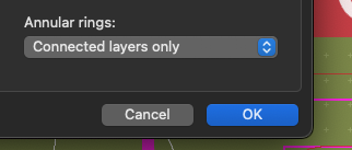
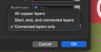
You can remove the annular rings on the inner sides, the outer annular rings are required.
I am working on proper documentation atm, and I am also getting additional feedback as you still need to take drill wandering in consideration with regard to the clearance.
Out of curiousity, what happens when vias are smaller than 0.5mm?
I have ordered several boards with 0.4mm vias (0.2 hole / 0.1 ring) and rarely have issues.
@Thea, are the vias adjusted or does it just create additional risk?
Hi again everybody. I got a little clarification by email that I thought I would share here. The 0.1mm minimum drill size is of the smallest officially supported via is actually the finished drill size, after plating–so now things start to make a little more sense.
@Thea, I just need to know how much space I need to leave for clearance on the layers where the annular rings have been removed. It makes total sense to me that some separation needs to be maintained even if there is no copper officially present in the layer. To achieve this, I’m considering making a via stack that has different sizes in the connected and unconnected layers. It will be a little more complicated than just choosing the “Connected layers only” option, but I think it will let me be more explicit and get the best possible copper fill on the inner layers while respecting all the Aisler design rules.
Hi everybody. @Thea. I’m still waiting for the guidance on the clearance (to copper of a different net) we need to leave on an inner layer that has had its annular rings removed on inner layers.
Hi again everybody,
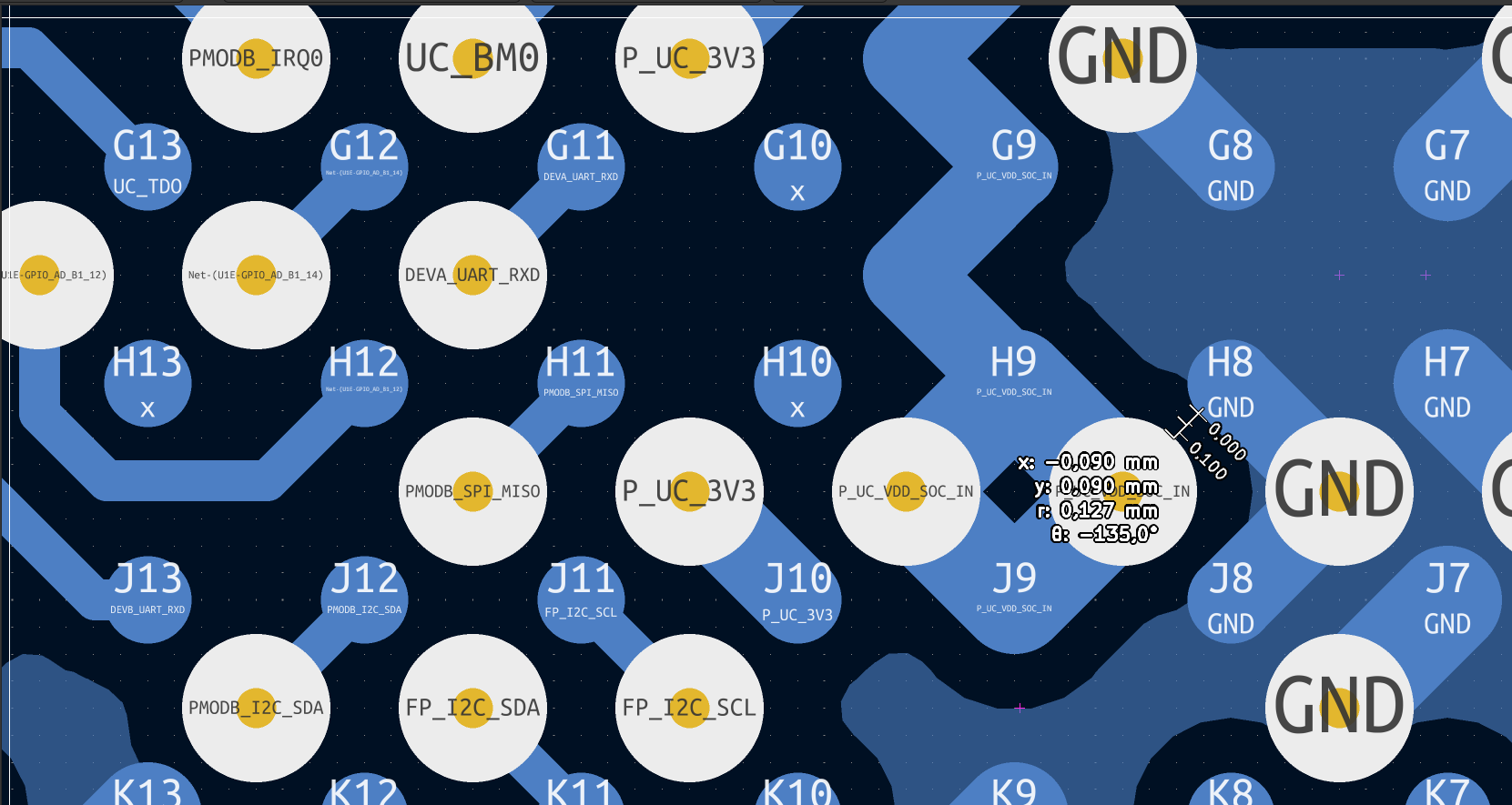
I’m hoping we can come to some kind of a conclusion on this issue, and thought that it might be helpful to show some real geometries from a board I’m developing now and stimulate the conversation. As I mentioned before, the BGA I need to work with has a 0.8mm ball pitch. I’ve reduced the pad size down to 0.32mm, which is still within the manufacturer’s recommendations. The minimum via size in Aisler 4L is 0.5/0.1mm, but for now I am sticking with 0.55/0.15mm (because the extra 0.05mm is not nearly enough to get traces routed out OR get closure of planes on internal layers anyway). As @Ondre pointed out at the beginning, KiCAD now has “smart” via stacks that will optionally remove annular rings automatically from unconnected vias on internal layers.
There isn’t too much margin, but this via/pad geometry allows me to maintain separation of >0.125mm between nets on external layers.
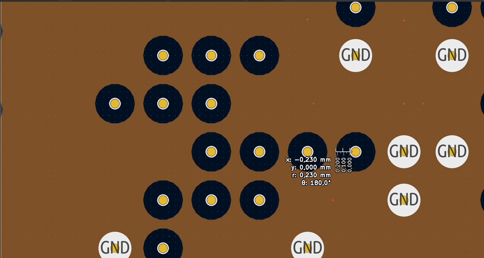
Now, with the annular rings removed, I have closure of the plane on my ground layer! I’m using the default Aisler 4L design rules (downloaded from the Aisler github, with a few of my own net classes added) and KiCAD 7.0.11, and it seems to me that KiCAD is adding a small sliver of an annular ring representing the wall thickness of the plating of the via, and the net separation between the barrel of the via and the ground plane 0.230mm. That seems quite reasonable me to account for registration errors of the drills, dispersion in the hole size, plating, etc. and still maintaining 0.125mm between copper of different nets. I’m not 100% sure where 0.230mm is coming from, I think it is a combination of a few things…
The situation on the power layer is similar. Good closure of the various power planes, and 0.230mm of separation between the nominal “barrel” of the via and the power planes.
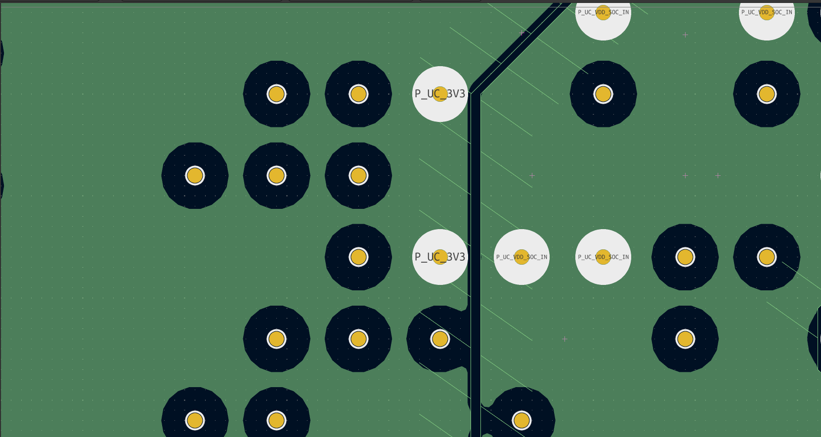
On the secondary component side, we have a similar situation, with a separation of >0.125mm being maintained between all unrelated copper. It is a big pain for me that between any two vias legal at Aisler, adjacent in the ball grid, it is impossible to route out even one signal, but that’s life, and there are ways to deal with it ![]()
I’m not sure how I would specify the minimum separation between via and plane on internal layers with annular ring “removed” if I were in Aisler’s position, but the resulting 0.230mm looks pretty reasonable to me…
I hope this was helpful. I’d love to get this figured out before Easter holidays. Have a great weekend everybody.
Regards,
-Kevin
FYI @kevin137 I have built several boards with 0.8mm pitch BGA using Aisler 4L. I’ve used 0.35mm and 0.32mm pad size with 0.40mm and 0.45mm vias and 0.2mm drills.
I do ocassionally get bad boards but this is caught by their smart tests. So, if you don’t need perfect yields then maybe you can use smaller vias. I’m curious what Aisler thinks about this.
We require a keepout of 265µm from the via barrel.
Hi @inc ,
Did you remove the annular rings from unconnected nets on inner layers in your designs?
I’m trying to come up with a geometry that’s 100% legal with Aisler and still works for me on this design–it looks like removing the annular rings will help me do it. If I needed to route out just one or two more signals from inner balls, I would need to change provider because I would need to be able to route signals between vias. I like Aisler’s service and business model, so I’m giving my best shot.
-K
Hi @Thea,
Just to be absolutely clear: 265µm from the center of the via, from the inner surface of the via barrel, or from the outermost ring of the copper of the barrel?
-Kevin
Outermost ring of the copper barrel.
Ok! Thanks for the clarification.
If I change the copper to hole clearance, whether per net or globally, to 0.28mm, I get 265µm from the outermost point of the copper barrel. I did also have to drop the via down to 0.5/0.1, but I guess that is legal as well, so it looks like there is a 100% legal solution to get what I need.
I can’t close this issue since I didn’t open it, but I’ve found a solution thanks to the Aisler team. Thanks everyone. Have a great weekend!

1 Like