Introduction
We’ve been offering our 4-layer 0.8 mm PCB pool for a while now (as of October 2024, to be exact). The reduced height makes them ideal for space-constrained applications or for modules with castellated edges. We’ve also seen makers wanting to create M.2 modules using our pool, so let’s talk about the M.2 formfactors, mechanical requirements and limitations, and manufacturing tips, so you can use M.2 cards in your next project.
Note: This article describes the capabilities of our low-cost PCB pool, which can be used to build functional but not spec-compliant M.2 boards. Please contact our support if you want to build M.2 boards for commercial purposes. As we are working together with numerous partners, we can offer services like beveling and hard gold as well as other tool diameters required for spec compliance through a special production run in combination with an assembly.
About M.2
The M.2 standard was released in 2013 to transition from the mSATA standard as devices became more compact. M.2 added more form factors, both smaller and larger than mSATA, allowing for a wider range of applications. PCIe, SATA, USB, I2S, I2C, SDIO, DisplayPort, and UART, as well as control/status signals, are listed as supported interfaces, though not all of them are available on every M.2 variant.
And while the standard focuses mostly on Wi-Fi, Bluetooth, GPS, cellular, and SSDs cards/modules, people have built all kinds of modules ranging from FPGA over Machine Learning accelerators to LED Matrix.
Both LGA (Land Grid Array) and PCB card with edge connector types are specified. We will solely focus on the commonly used PCB card form factor.
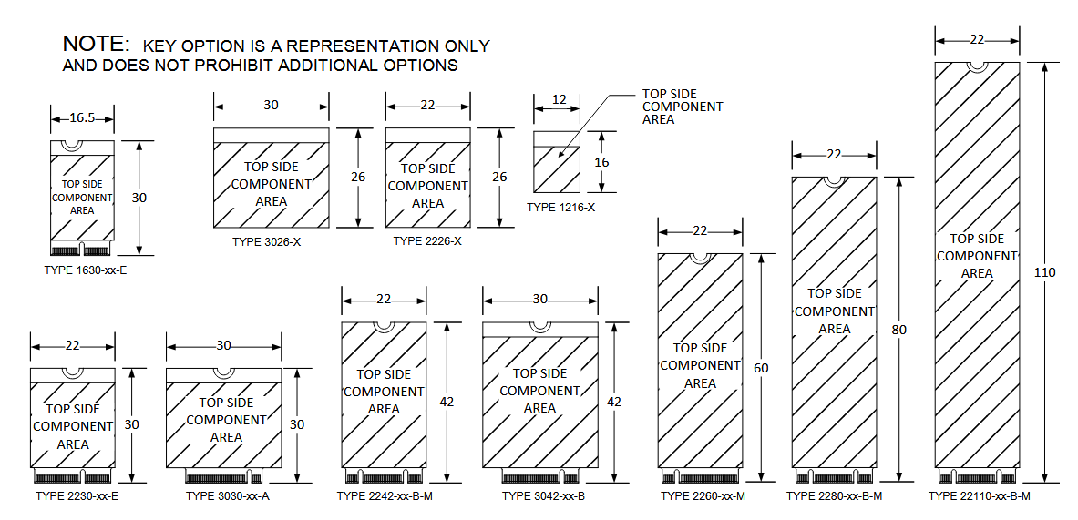
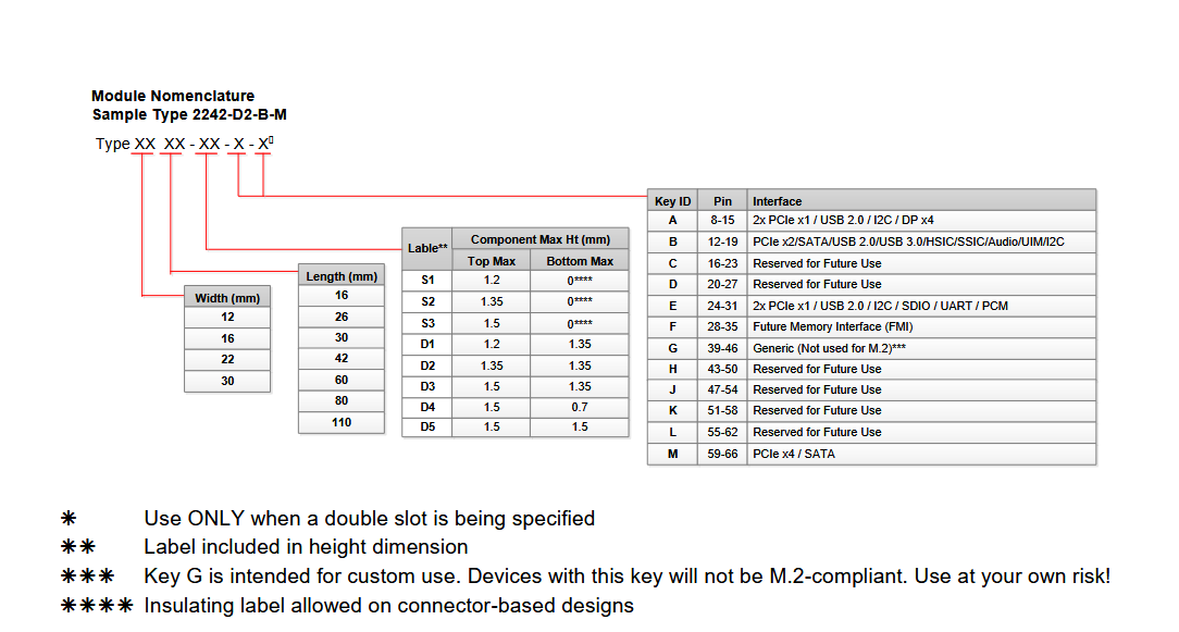
Naming convention
M.2 modules follow a specified naming convention that specify:
- Width & length of the module.
- Maximum height of the assembled parts on top and bottom side.
- The connector key(s) that specify function and pinout
Mechanical Requirements
This section lists the mechanical requirements listed in the M.2 spec and whether these conditions can be met when using the budget pool.
General Tolerances
| Parameter | Tolerance + | Tolerance - | Note |
|---|---|---|---|
| PCB Size Tolerance | 0.15 mm | 0.15 mm | |
| PCB Thickness | 0.08 mm | 0.08 mm | |
| Bevel Capabilities | 0.25 mm | 0.25 mm | |
| Drill Capabilities for Module key | 0.05 mm | 0.05 mm | |
| Radius listed in Fig. 16 | 0.5 mm + 0.15 mm | 0.5mm - 0.15 mm | |
| PCB Surface Finish |
PCB Thickness & Bevel
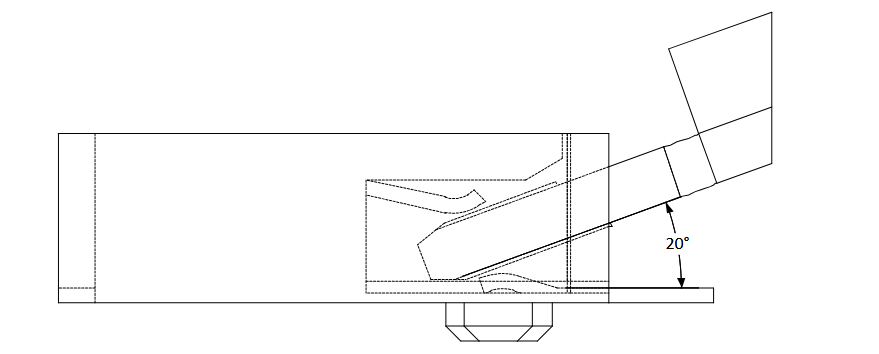
The M.2 spec specifies a PCB thickness of 0.8 mm ± 10%; this requirement is met by our fabrication processes. Bevels of 20° ± 5° which aid the mating process by reducing the mechanical stress, cannot be manufactured in our budget pool. They can, however, be left out at the expense of spec compliance and higher mechanical wear, which should not be the greatest concern for hobbyists.
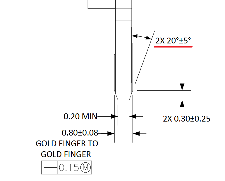
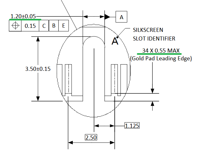
Key and Pad to Leading Edge Clearance
A slot width of 1.2 mm is specified for the “key” that prevents the insertion of M.2 cards in a connector that uses another “key” and thus are inoperable due to different pinouts. This slot will be realized using our 1.2 mm nibble drill, whose tolerance falls within the requirements.
A maximum pad-to-edge clearance of 0.55 mm is given, we recommend a clearance of 0.3 mm, as this would be the nominal length of the bevel and the minimal copper-to-edge clearance in accordance with the 0.8 mm 4-layer design rules.
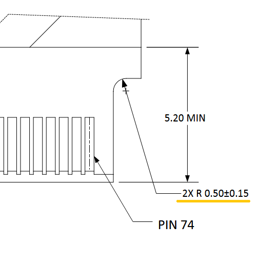
Radius between edge connector and component area
A radius of 0.5 mm ± 0.15 mm is specified for the area where the edge connector goes over to the component area. Using our 1.8 mm milling tool for PCB outlines, the smallest possible radius is 0.9 mm. While noncompliant with the specification, this did not pose issues during our testing, as the PCB did not interfere with the connector.
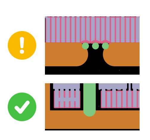
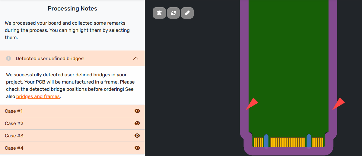
Placement of PCB tabs
The PCBs are connected to the production panel using breakaway tabs, (we also call them bridges). These tabs are placed automatically using the software pipeline that processes the production data.
As the software is (unfortunately) unable to recognize the edge connector, it is required to mark the desired placement of these tabs in your design files. Please refer to our documentation on how to do this: Custom Tabs and Panel Frames
Design Checklist
Before ordering your design do these steps in your PCB design tool:
- Check footprints and schematic
- Run a Design Rule Check
- Place the marker for the PCB tabs
After uploading your design, verify in our PCB viewer that:
- The placement of the PCB tabs/bridges has been processed correctly
- The Key is marked in a blue color, this indicates that we will use the nibble drill
Please also address any issues or warnings we display in the processing notes, contact our support if you require help.
IMPORTANT NOTICE
AISLER assumes no liability for design assistance provided by this appnote/guide. Engineers/designers are responsible for their design.