Please Note: This Guide is only applicable if you already installed the Altium Push Outjob. In case you are installing it for the first time follow our main guide.
Step 1: Update Publishing Destination Settings.
Head to Preferences → Data managment → Publishing Destinations → AISLER Push.
Click on Edit Connection
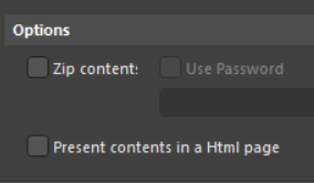
Under Options unselect the Checkbox Zip content.
Save the Settings.
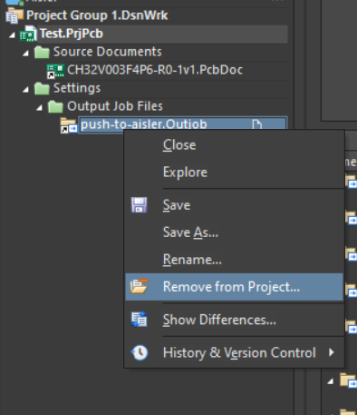
Step 2: Removal of the old Outjob from the Project.
Navigate in your file structure to
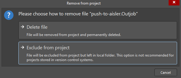
Select Exclude fom project.
Navigate to the file location and save the Outjob at a different location. In most cases the ODB++ is the better choice but during the transition period there might be things that not work, thus keep the Gerber.
Using “Add Existing to Project…” on the “Projects Panel”, import the Outjob configuration to your project and assign the layout you would like to submit.
Make sure your PCB file and Outjob are in a project, the export will fail otherwise.
Generally I really like the idea of switching to ODB++, and generally the whole push-to-aisler workflow for Altium is REALLY nice!
Unfortunately, I’ve recently run into quite some problems with this new method of getting my designs from Altium Designer into your online tool. First of all the fact that no kind of cut-out or in-board routing is possible is pretty much a non-starter and forced me to fall back to manual gerber export anyway (for which there is no longer any documentation, correct me if I’m wrong).
A second issue I ran into with both approaches was the length limit of designators. With multi-channel designs in Altium it quickly becomes very hard to keep designators below the required 6 characters of length without performing a board-level re-annotation of the whole project (which is a lot of work for a quick prototype).
In my opinion the most easy solution would be to require users to create the board shape on the designated ‘Board Shape’ layer in Altium, and then export that layer instead of the internally generated Board Outline Layer. For in-board milling the ‘Route Tool Path’ Layer should be exported as well by the output-job. Both those exported layers could then be combined in your online tooling to create the final board shape.
Hope this feedback helps you improve your tools even further.
We fixed the cutouts issue, our documentation was not reflecting that though. I updated the article now.
We tried the method of using a designated layer for the board shape but Altium still exported it to two different ODB++ profiles. But our import software pipeline is now updated and processes profiles to create the board outline.