On soldermask margin/openings

First, a look at the current situation

The AISLER’s Design Rule Rating of your PCB topic states that:

Soldermask openings should have the size of the underlying pad, as the openings are automatically enlarged by us.

Aisler’s custom KiCad design rules forbid soldermask margin override.

The Soldermask Opening Adjustment topic states that:

Our System assumes that optimized soldermask openings are larger than the copper pad. Square, Rectangular and Round openings can be optimized, irregular shapes will be left as is.

A potential problem

If I understand it correctly, polygons on the copper layers will not have the soldermask automatically moved back. This could results in issues, could it not? As stated in Soldermask Opening Adjustment:

A misalignment of the soldermask might cover up parts of a pad, , resulting in less space to mount a component.

Should it be concluded that in general, a custom soldermask margin is discouraged but, in some cases, it is required?

If this is the case, perhaps the custom design rule should result in a warning?

The consequences of a custom soldermask margin

What happens when the design rule is ignored and a custom soldermask margin is requested/ordered? Are there any disadvantages or potential problems related to this given that the custom margin is large enough, e.g. >20µm?

Following these questions, why is the custom soldermask margin forbidden in the first place? Is it to simplify PCB design as the designer does not have to keep the soldermask margin in mind or prevent too small margins?

Use case

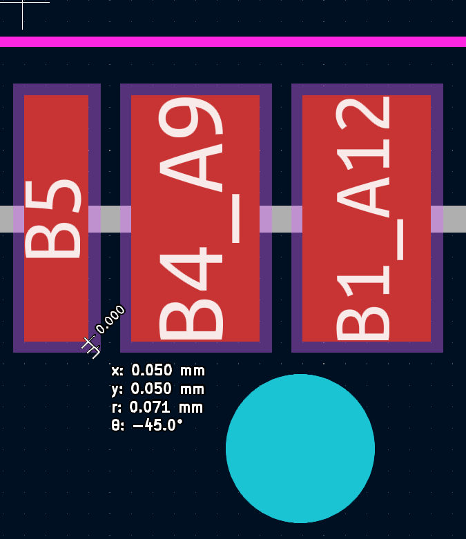
In a project, I have a NPTH that is very close to some pads (185 µm). In order to comply with Aisler’s 250 µm constraint, I cut parts of the pads’ corners.


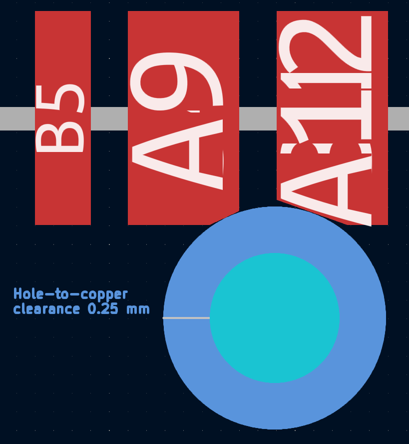
Now I’m wondering if I need to apply a custom soldermask margin despite the design rule.

The manufacturer of the component has the following custom soldermask margin.

Looking forward to your insight,
Matthias

Hi Matthias,

Thank you for the heads-up, I recently overhauled our design rules and forgot to adjust the wording for the soldermask openings. You can apply a custom soldermask opening if so desired, but due to our implementation the custom rule will not be applied to pads in copper planes, this is not much of an issue as most of the pads in copper planes are power devices which have a larger land pattern to begin with, which compensates for a possible misalignment.

I will update the wording and custom design rule for KiCad.

I don’t quite understand the following:

You can apply a custom soldermask opening if so desired, but due to our implementation the custom rule will not be applied to pads in copper planes

  • What is meant with the custom rule?
  • What is the current handling for non-regular shaped pads on copper planes? Is it different from e.g. rectangular pads?

I look forward to the wording and DRU updates, hopefully they’ll clear up my confusion.

Hi @Thea, has there been any progress on this? It looks like the new board specific PCB design rules no longer mention the automatic opening but the Soldermask Opening Adjustment has not changed and neither has the KiCad DRU repo.

Specifically, I’m interested in the following:

  1. I have components where the recommended land pattern defines soldermask that overlaps the pad, will this be respected or a problem?
  2. I have custom shape pads that need soldermask margin
    a) will adding my own margin be respected
    b) if I do not add margin, will you add it automatically
  3. I have rectangular pads that need custom soldermask margin, will this be respected.

Best regards

Matthias,

it seem you have the same problem with USB-C connectors that I have. In several recent Aisler designs, I used normal pads and ignored the warning resulting from the too small distances by the board viewer. Boards were successfully produces despite.

1 Like