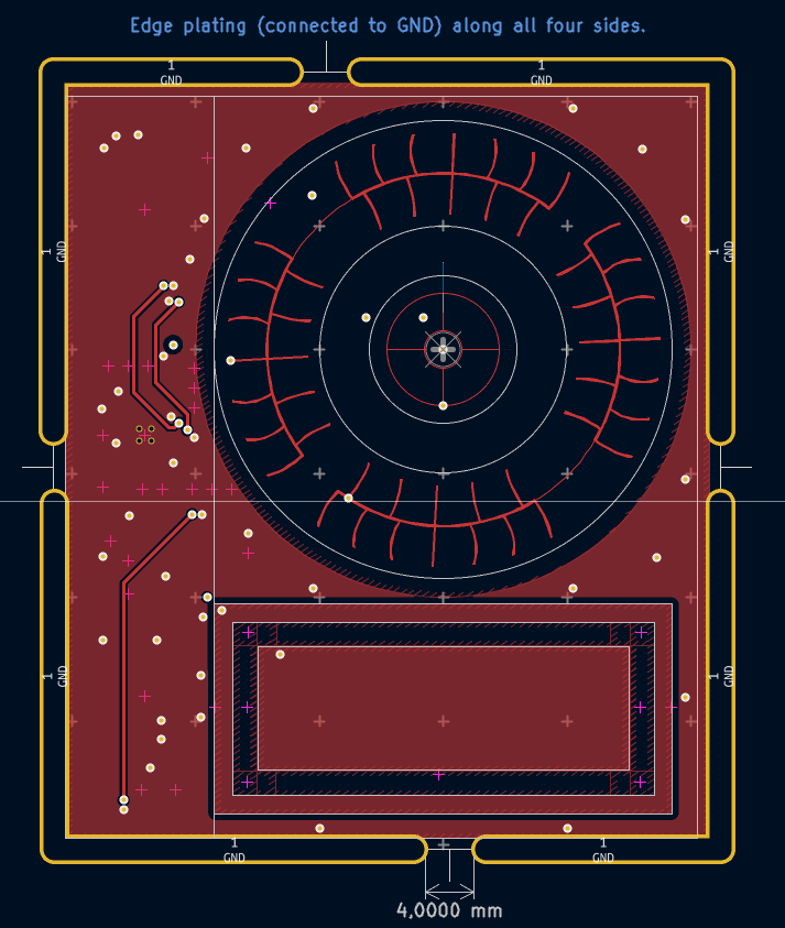
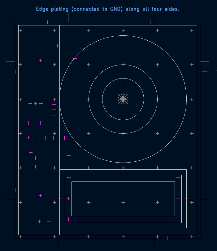
In order to reduce the ESD risk on a capacitive touch sensing board, I would like to implement edge plating on the design in order to surround the edges on all four sides.
I am aware that a fully plated edge around the whole rectangular PCB-perimeter is not possible due to the bridges/tabs that connect the PCB to your frame.
What copper clearances around the board edge do I need to apply that you know what planes shall be connected to the plated edge and which not/be pulled back?
Is there anything else I need to keep in mind in order to prototype this on your 4-Layer-ENIG pool?
Looking forward to hearing from you.
Best regards,
Yannik
I thought it might be helpful to provide some further information of the current state.
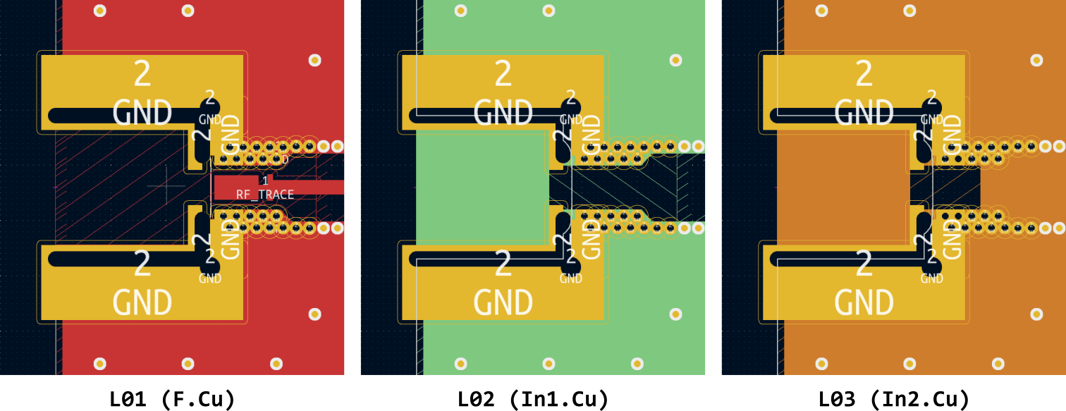
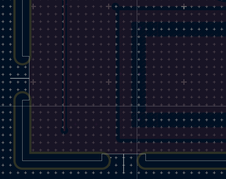
Currently, I pulled all areas which shall not be connected to the plated edge/side back by at least 300 micron specified in the 1.6 mm 4 Layer ENIG design rules.
Layers which shall get connected to the side plating extend fully to the board outline.
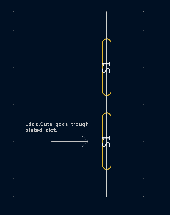
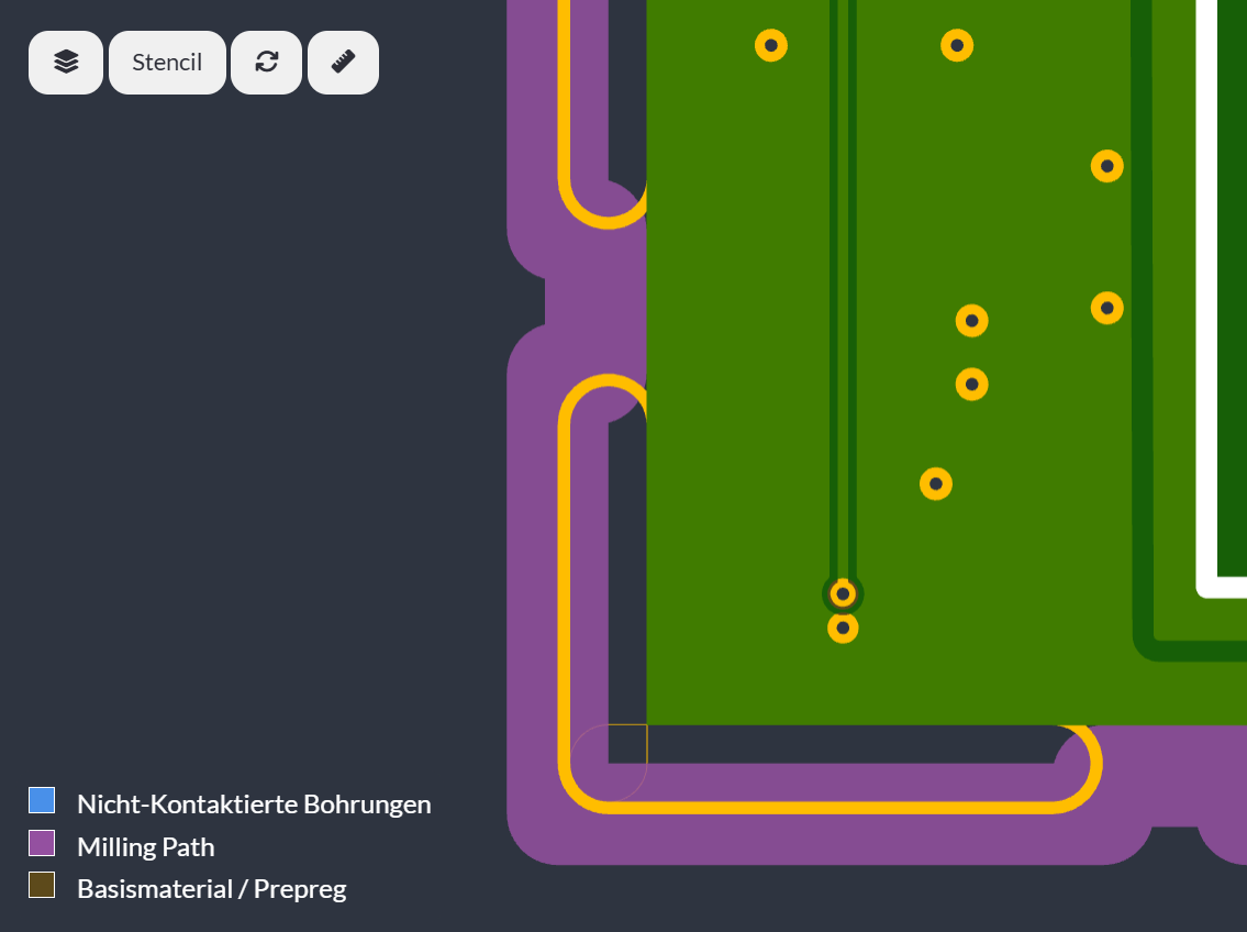
We mill the PCB outlines after the plating during the manufacturing, so you need to place plated slots in your design and then run the board outline through the plated slot. A wider width of 1.8mm will make the plated slot easier to manufacture.
I am afraid though that the extensive use of slots to achieve all around plating would lead to a non-producible design. Most of the board outline would be milled away at an early manufacturing stage.
Do I need to interrupt the plated edges more frequently for it to work?
As of now, the design triggers a “critical use of elongated holes” warning and requires contacting support, though the slot width is 1.8 mm (no need for nibbling, in accordance with Plated and Non-Plated Slots).
4mm should work, I spoke with the production folks again, they wanted to clarify that the process is not recommended for large quantities of boards, so we will manufacture a few dozens using this process but not hundreds. If you require more boards, we will use have to use a different approach.
Hey Thea,
just to keep the topic updated:
I submitted a support ticket, so that someone can look over the proposed design and eventually (hopefully ) clear it for manufacturing, as it requires manual clearance because the total PTH slot length is above the granted 75 mm.
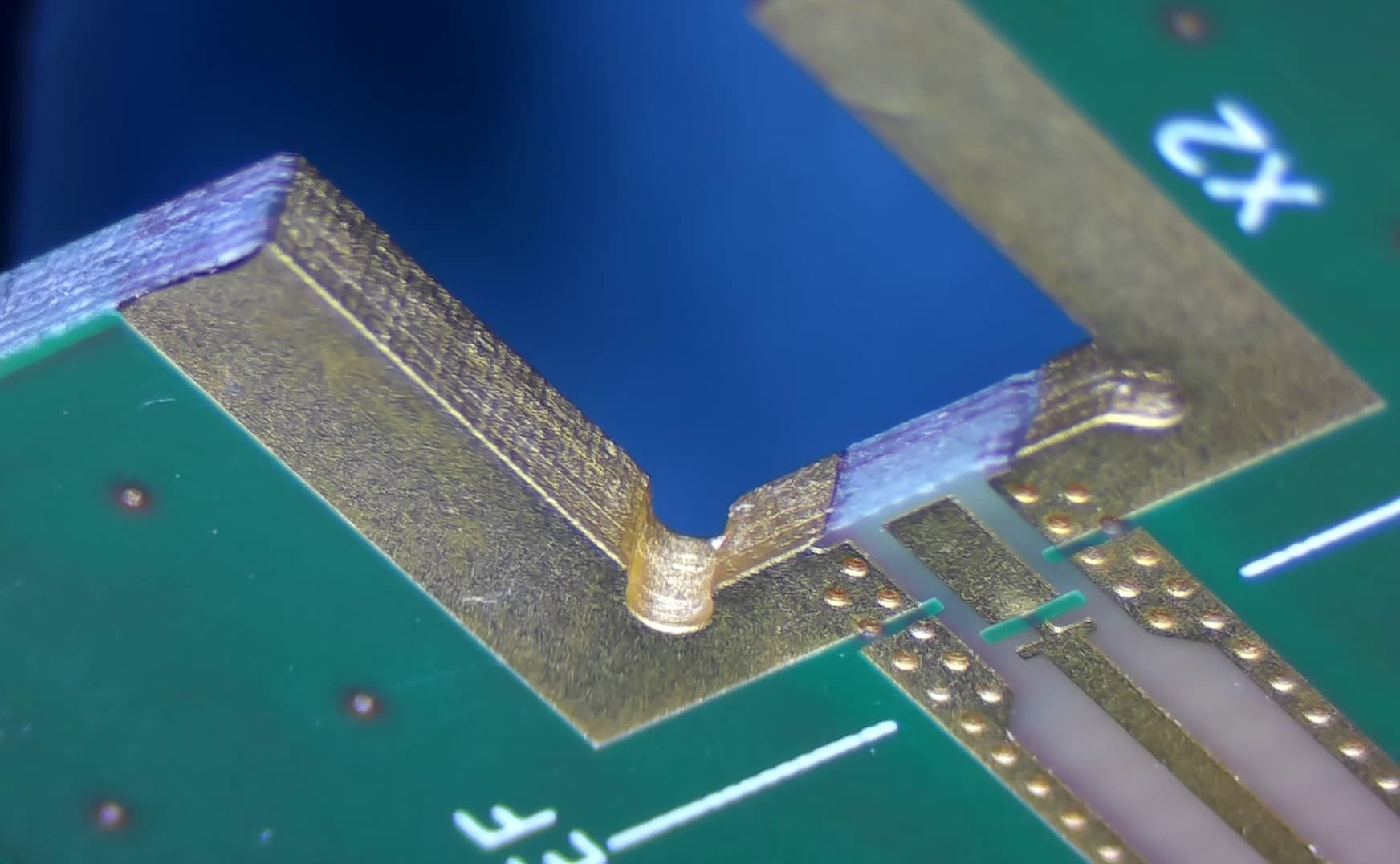
I will provide a picture of the boards if they arive so that this thread may be somewhat used as a future reference.
If it turns out to be functional, I might post in the “Made with AISLER”-section as well; we will see…
It’s been a while and unfortunately, I have not received a reply to my ticket.
Having called the support team twice (this Monday and the Monday before), I had two very kind conversations, in both of which I was told that a colleague would get in touch with me the next day. That unfortunately never happened.
I would really like to produce this with you - to prove to myself and my colleagues that its perfectly doable to get prototypes produced here in Germany for a decent fee.
Sorry for the delayed response, the one-day response was something I told my coworkers when they asked me about your issue. Unfortunately, the past few days were super busy for me and I did not get the chance to answer so far. I had a brief look at the project and the bridges don’t line up yet, could you please review their position? My schedule is more free tomorrow, I will give you a more detailed response.
thank you for providing more context, that helps me understand, why it took longer.
Are you sure that the specified bridges do not line up in the latest revision (Rev. 7) as both your board viewer and KiCad show them exactly opposite of each other?
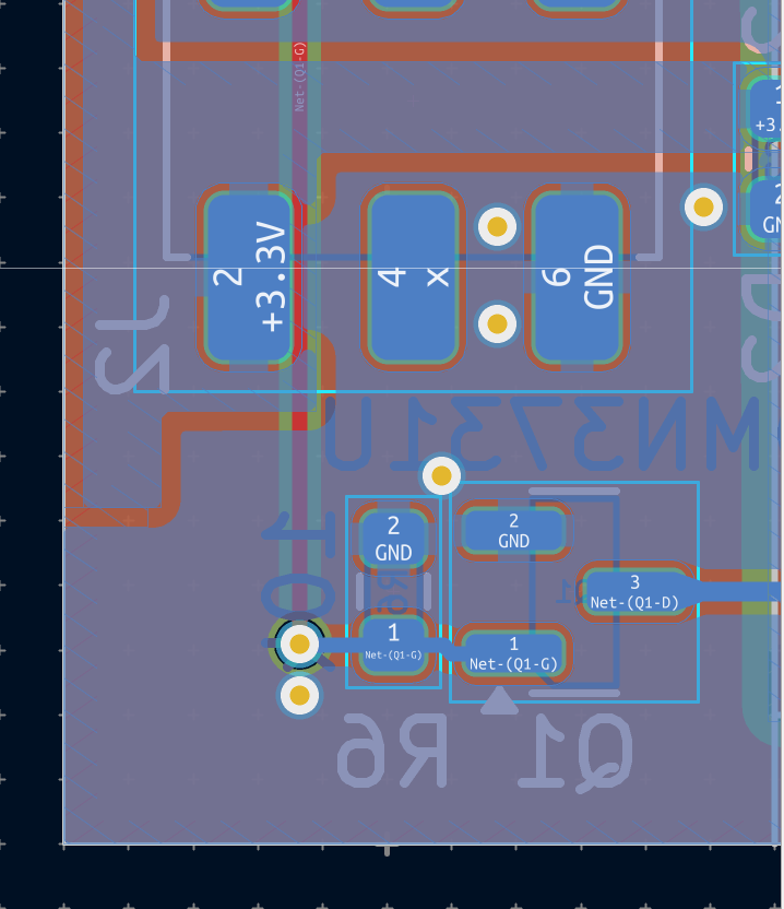
Okay, looked at it more closely again. The bridges are at the right position, but we would mill trough them at the time. Could you please upload the KiCad PCB file directly So I can check how you drew the board outline?
I guess the problem you are mentioning is caused by these parts in the outline. They were intended to force the milling tool onto a path that removes more from the PTH-Slot, so that just the plated edge remains: