Hello everyone,
Here is my first ever forum post ever about pcbs. ![]()
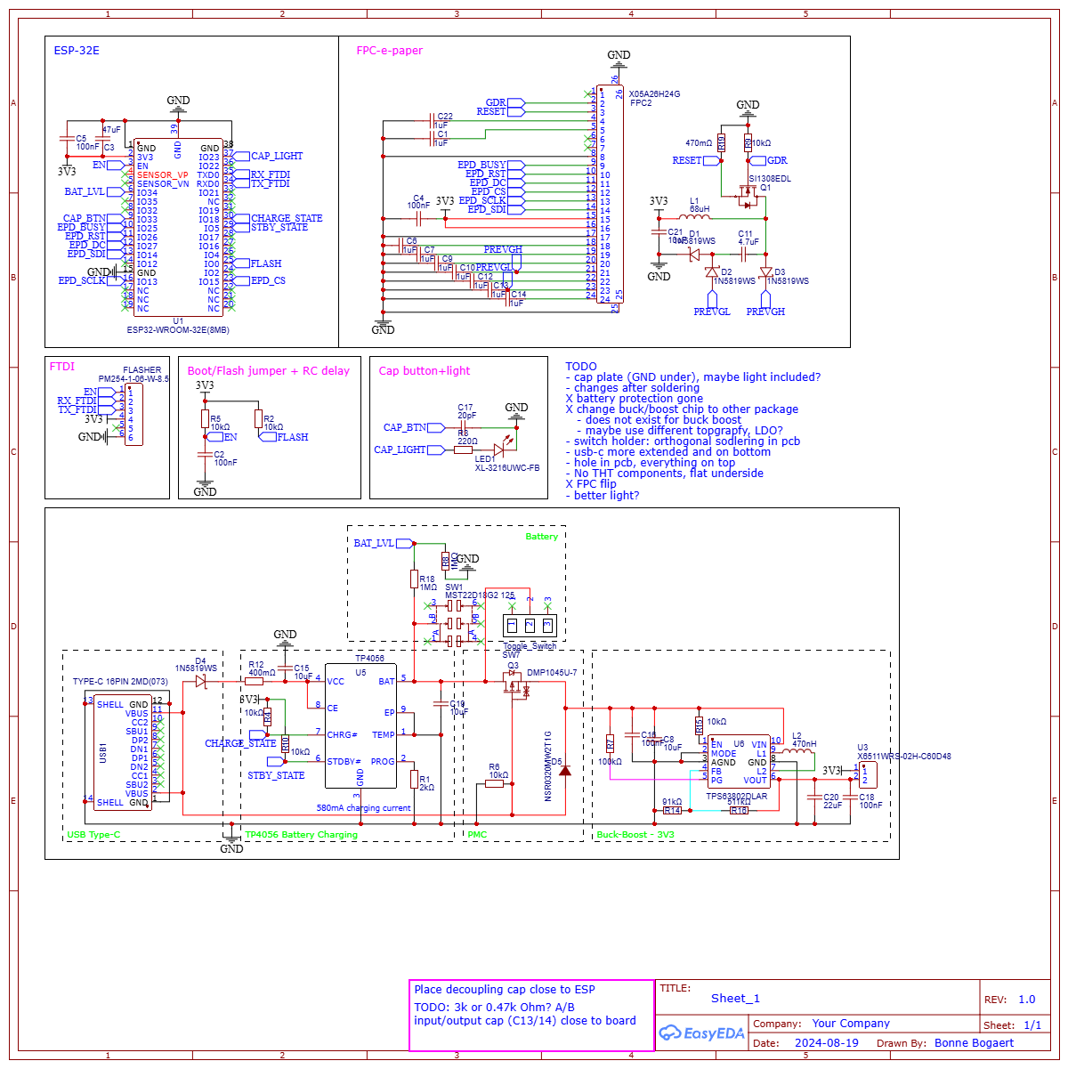
I am designing some kind of wall frame with an e-paper screen with an esp32 to show weather, calendar, goals, todos connected to an app. See first picture for backside.

As you can see, it has an usb-c port on one side, a central bottom piece with a capacitive button that triggers when a finger presses the wood above.
And on top, I want a toggle switch to turn on/off the power.
I have two questions:
- Why cant Aisler build the PCB like this with the holes on the side, the drill should just go there right and drill? JLCPCB doesn’t complain about this.
- Can someone check my designs?
 Since I have limited experience, also for the power part between USB and battery. Is there another way to minimise power usage so the battery can last at least a half year?

Thanks in advance!
I appreciate any help