Abstract
This circuit appnote outlines the factors that must be taken into account in order to design stencil apertures that improve solderability and yield.
Introduction
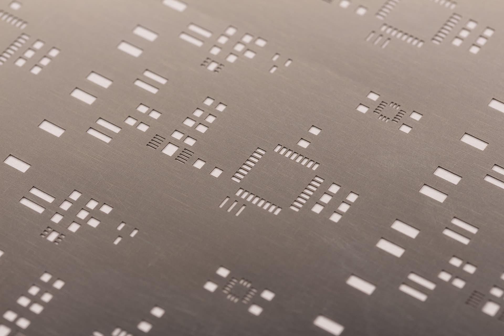
A stencil aperture refers to the opening in the stencil through which the solder paste is printed onto the board. Most stencils, like the ones we offer, are manufactured from stainless steel. Some companies offer polyimide film ones as well, and while they cost less, they also have a shorter lifetime and are generally more difficult to work with. Our prototype stencils are made using Japanese stainless steel with a thickness of 100 µm to also support smaller components.
You have to design the stencil opening on the corresponding layers in your EDA tool when you want to order a stencil from us. You can use the stencil button in our PCB viewer to inspect if the data has been processed correctly.
| EDA Tool | Top Side | Bottom Side |
|---|---|---|
| KiCad | F.Paste | B.Paste |
| EAGLE | 31 tCream | 32 bCream |
| Fusion360 | o3 tCream | o4 bCream |
| Target3001! | Layer 19 Solder Paste Top | Layer 5 Solder Paste Bottom |
The paste layer(s) are “negative”, so features drawn on them will be cut out of the stencil.
Impact of aperture design on manufacturability
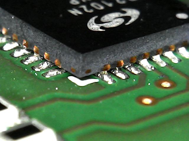
The area of the opening and the thickness of the stencil determine how much paste is deposited. This volume needs to be controlled using the aperture design. Too much, too little solder paste or the wrong aperture design can lead to solder defects.
Besides the more obvious effects of shorts between component leads due to too much paste or unstable solder joints due to too little, one also has to take the properties of the paste during reflow into account.
Large stencil apertures in general are difficult for multiple reasons. During printing, the squeegee is not supported by the stencil and can scrape on the PCB surface. Further, during reflow, large volumes of solder paste form big “blobs” which can lift the component, in addition to this, the flux in the paste, which outgases as fumes, can shift the component from its original placement.
An image of such a solder defect is shown below:
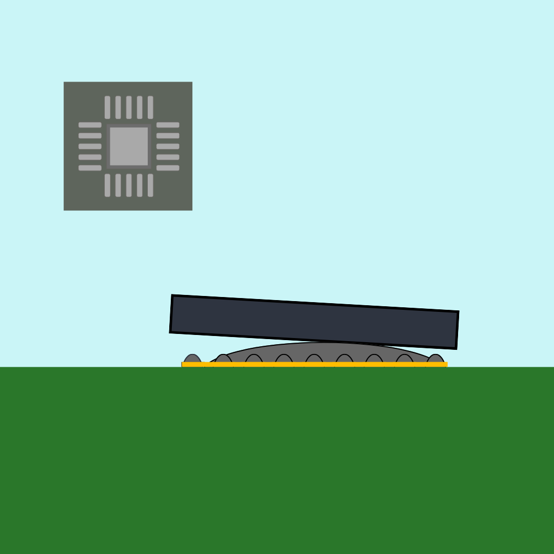

This effect can be prevented by using a “window pane” design, which separates the bigger opening into multiple small ones, reducing the volume of solder paste and allowing the fumes to escape.
Aperture Design
The datasheet of components often recommends stencil apertures for a given stencil thickness. These provide a good starting point but shall be verified in your particular process and adjusted accordingly.
Minimal Size
The minimal aperture opening is a function of the stencil thickness and used solder paste, thicker stencils or solder paste with coarse solder particles will require larger apertures.
To ensure proper release of the paste during printing, rectangular apertures shall be able to fit a minimum of five solder particles in width and length, and circular apertures shall fit a minimum of seven solder particles.
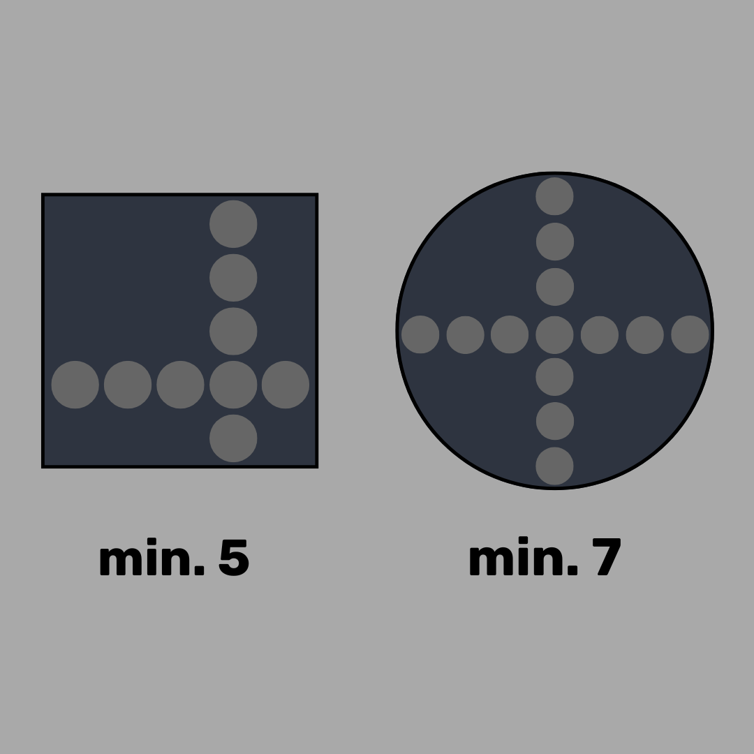
The solder particle sizes are grouped in “types,” with higher numbers denoting smaller particle sizes. Only Type 3 and finer pastes are broadly offered nowadays. Type 4 is sufficient for most components, finer paste will incur higher costs due to the stricter qualification and lower yields during manufacturing.
Solder particle size classification after J-STD-005 Table-2:
| Type | Less than 0.5% larger than | 10% max between | 80% min between | 10% max less than |
|---|---|---|---|---|
| 1 | 160 µm | 150 - 160 µm | 75 - 150 µm | 75 µm |
| 2 | 80 µm | 75-80 µm | 45-75 µm | 45 µm |
| 3 | 60 µm | 45-60 µm | 25-45 µm | 25 µm |
| 4 | 50 µm | 38-50 µm | 20-38 µm | 20 µm |
| 5 | 40 µm | 25-40 µm | 15-25 µm | 15 µm |
| 6 | 25 µm | 15-25 µm | 5-15 µm | 5 µm |
| 7 | 15 µm | 11-15 µm | 2-11 µm | 2 µm |
For the calculation of the aperture, we take the largest permissible size that comprises the majority of the paste. For Type-3 this would be 45 µm, for Type-4, 38 µm.
Example:
For rectangular apertures, the smallest supported when using Type-3 paste would be 5*45 µm = 225 µm or 0.225 mm.
Or 7*45 µm = 315 µm or 0.315 mm for circular apertures.
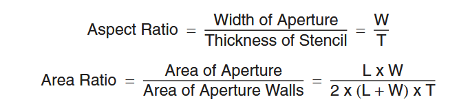
Aspect & Area Ratio
IPC-7525 defines formulas for calculating the aspect ratio and the area ratio of the stencil aperture for reliable paste release. An area ratio of >0.66 and an aspect ratio of >1.5 should be reached. If these values are not reached, the aperture should be adjusted.
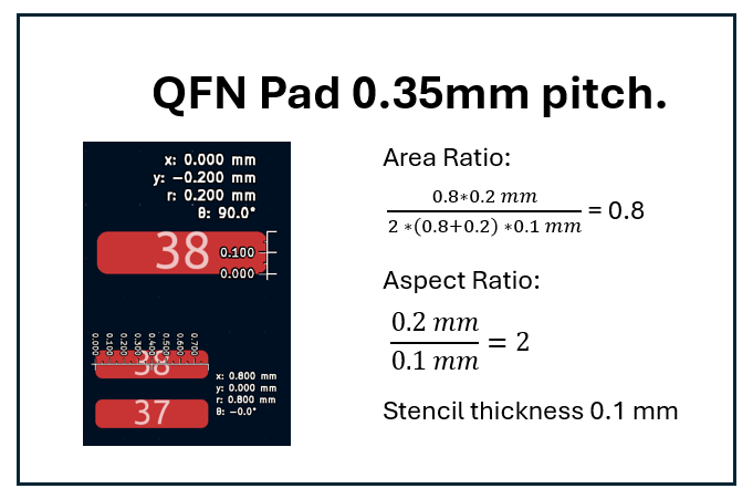
However, the 100 µm thick stencil offered by us supports even challenging apertures like this 0.2x0.8 mm pad of a QFN with a pitch of just 0.35 mm. Thus, adjustments won’t be necessary in most cases. The example calculation below indicates that there is a robust margin to the minimum recommended values.
Rounded Corners
The corners of stencil apertures should be rounded to ease paste separation and avoid leftover paste getting stuck in the corner of the opening.
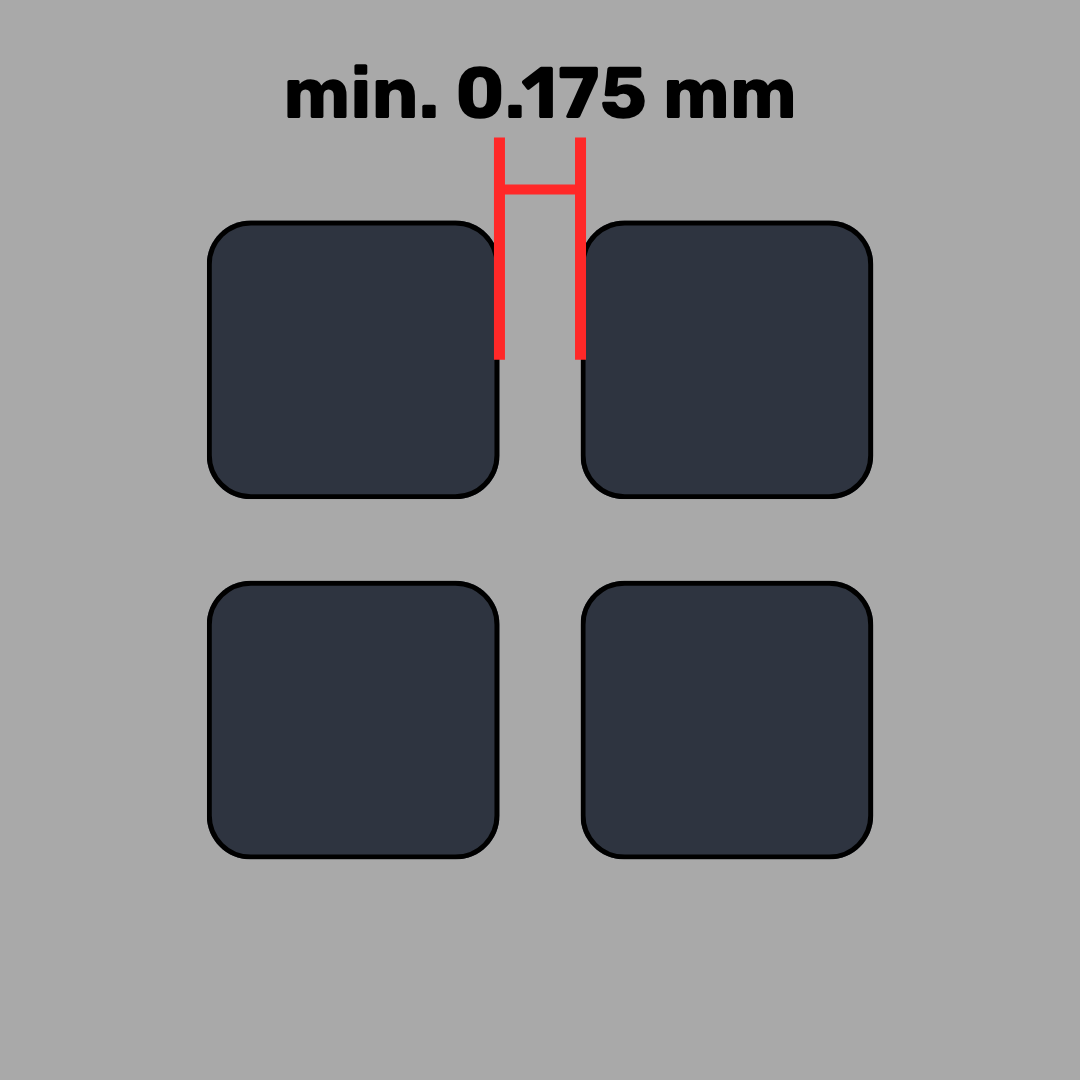
Stencil Bridge
The minimal width of a stencil bridge is 0.175 mm.
Window Pane Opening
Large opening shall be divided using a windowpane design, the solder paste should cover 50-80% of the pad area, ~65% is recommended.

IMPORTANT NOTICE
AISLER assumes no liability for design assistance provided by this appnote. Engineers/designers are responsible for their design.