2-Layer HD stackup clarification

Hi all,

I am confused by different information rgd the AISLER “Beautiful Boards HD 2L” stackup, specifically the core material and respective parameters.

So on the one hand, according to

the core material is Technolam UV-Block FR-4-86.

On the other hand, according to

the core material is Iteq IT-158.

So which is it? Or am I misreading something?


I am specifically interested in correct parameters for:

  • Permittivity
  • Loss Tangent

(as well as final/processed thickness), but above 2 different materials do have significantly different parameters.

Any hints/helps greatly appreciated, thanks!

/Tobias

1 Like

Hi, sorry for the confusion. I will ask internally for the most up-to-date information and change the article accordingly. I maintain most of our documentation, and sometimes things are missed when updating it simply due to the fact of how many articles there are.

What I can say already is that our final/processed thickness has a variance of ±10% which is a typical value in the industry.

1 Like

thank you so much for digging! also thickness!

rgd docs: yeah, I totally understand, lots of work. I also have some to maintain;)


fwiw, because of the “outdated / incorrect” issue, nowerdays I usually generate docs from code. and then maintain and CI test the code. this removes a couple of traps and work.

in an ideal world, I’d git clone an Aisler GitHub repo with OSS Python code for both the stacks and materials definitions …

would be interesting to hear your thoughts, what are people/pros in the hardware community usually do? I mean with all this PCB stuff. I am a SW eng. and HW is a complete new world for me. so pls excuse my maybe silly questions;)

I, personally, like to document things using Markdown. The forum format has been chosen before I started my job here at AISLER, mainly because it is easier to engage with people and get feedback directly.

Markdown is great! Standard flavor or GitHub flavored. The latter is even better. And yeah, engaging people is super important I absolutely agree. I am using it a lot as well. On GitHub and for doc centric stuff, including for generating other formats (PDF…, RFCs, …), but I probably use Sphinx even more, I am just a Python guy;) But I’m using it even for non-Python, or even business oriented docs as well. Love being able to just use/embed Godot and the kitchen sink;)

fwiw, here is a glimpse of the Aisler stack stuff as I am using it

docs:

code:

Did you hear anything back already?


One more Q: does Aisler offer impedance testing - in general (for production runs) and/or for prototype runs (“Beautiful Boards”)?

I could add a microstrip transmission line isolated/separated from the actual stuff onto my PCB, and then verify and know for sure if my assumptions add up based on values measured by Aisler for a “known target” (the microstrip line designed for 50 ohm or 100 ohm).

“Continuous Testing” fully automated, always and end-to-end is a standard best practice in SW development these days. I’d love to do that with HW as well …


here is another discrepancy: the KiCad PCB template at

has yet different values than the PCB stackup docs here - for both Dk of core, and for Dk of solder mask, and it seems to use the raw/unprocessed copper thickness, not the processed thickness

mmmh. so there are 3 sets of claimed values, and the actual real values is of course unknown to me … which ones to choose … :wink:

1 Like

Hi, I will notify you when I hear back from the manufacturing people. We do offer impedance testing on production runs, but not when using the prototype pools. Single design panels can be controlled much tighter than the multi design prototype panels.

I believe the best software analogy would be that some tests cannot be implemented in a software container, and only be tested on the actual embedded device.

1 Like

Thank you so much!

Also for the explanation and comparison with SW dev =) I get it.


fwiw, I’ve decided I will not fully rely on / trust any documentation, but measure and test myself.

I’ve ordered me a 6 GHz 2-port VNA and a professional RF Prototyping and Test Fixture that comes with complete characterization, data, PCBs and Gerber files (!).

So once I have that, I can verify their published data “at home” using my VNA, and then have PCBs manufactured via Aisler using their Gerber, and then measure those.

Once I have that, I can change the PCB to my actual stuff, reusing the same test fixture and equipment, and then go “step by step”.

Always have a “known good” and “reference point” is also a SW test strategy … I am optimistic I can reuse that;) Will see, I am new to all of this stuff.

Hi :wave: , it took quite a bit longer than anticipated before got feedback from the production engineer. We exclusively use Technolam UV-Block FR-4-86 for our two layer PCBs.

1 Like

Thank you so much for digging and for coming back on this. Very much appreciated!

Also for coming back at all, as I am just some random nerd at this time, obviously not some “big fish” with big numbers of PCBs coming around;)


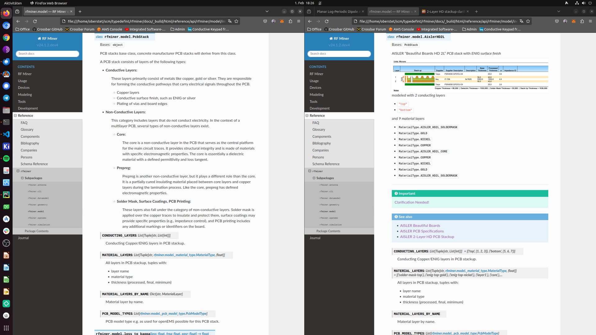
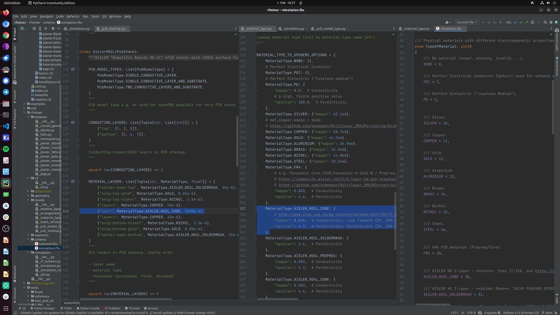
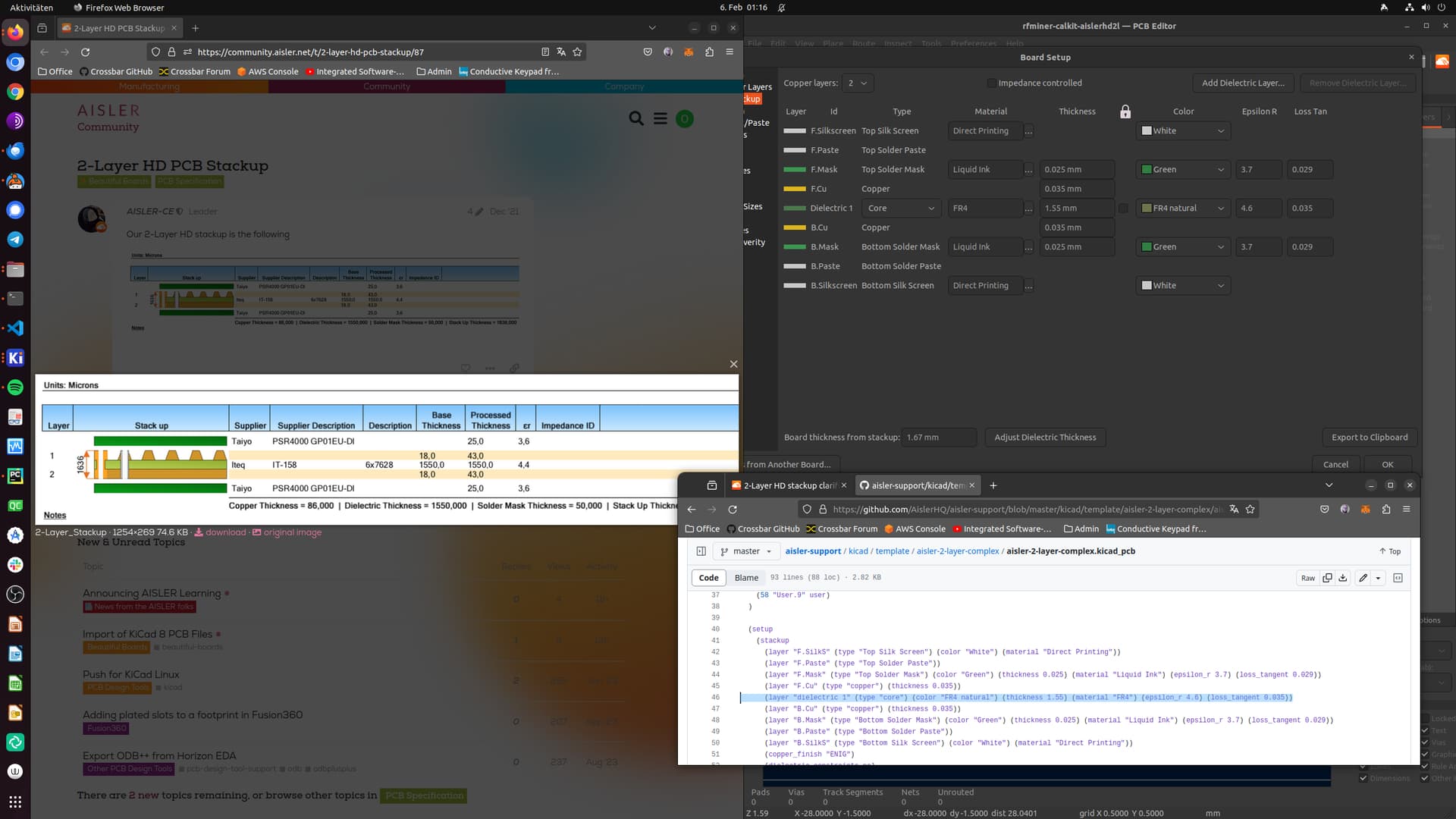
So according to the datasheet, and the other information on the stackup, the 2-layer AISLER stack has a dielectric layer with

  • Thickness (processed) 1550um
  • Permittivity 4.7
  • Loss Tangent 0,020

I will add this information into my modeling code.

Obviously, having consistent information in the AISLER docs would be nice and great as well :wink:


Now, I am still “getting into” all of this, and gain experience, try out different tools, methods and also manufacturers, both PCB and PCBA, and for the different boards my device needs.

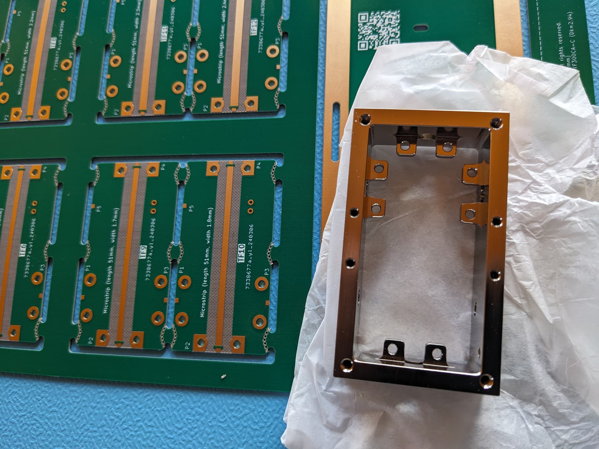
FWIW, for the antenna boards, I now have ready made first PCBs from a different source which I will use to validate / calibrate my openEMS models:

I haven’t done assembly and VNA measurements yet, so I should be careful, but for the antenna boards of my device (and those are just one of two types I need), above looks good - it’s using low Dk PTFE.

I will come back once I target the mentioned 2nd board type for the device, which will likely use a more “standard” 4-layer FR4, and PCBA is crucial for that as well, and I’d love to give that a try via AISLER!


thanks again, kind regards,

/Tobias