Important Note: 6 Layer PCBs have been discontinued
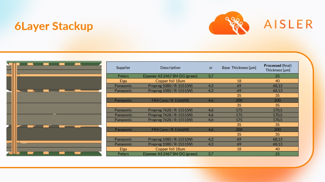
We use Panasonic Prepreg 1080 Type R-1551(W) (58.9 KB), Peters coatings and Elga Copper foil.
Important Note: 6 Layer PCBs have been discontinued
We use Panasonic Prepreg 1080 Type R-1551(W) (58.9 KB), Peters coatings and Elga Copper foil.
Nice, but much higher priority for me would be 1mm thickness in 2 or 4 layers. I would even prefer 6 layers in 1mm because 6 layers are mainly needed for fine-pitch BGAs and then miniaturization is the goal. PCB thickness contributes significantly to that.
I think this answer fits perfect to the Feature Request category. (👥 Feature Requests - AISLER Creative Community)
![]()
Hi, it is already there…
Argh… Only 2 links per post allowed. Here is the 3rd one:
There is an impedance table for 4L boards here:
I’ve found that table to be a useful reference. It might be helpful to provide a similar table for 6L boards to help verify calculations, even if it doesn’t cover all possibilities.
Thanks.
Thank you for providing an overview for the stackup ![]() . Are there any values for the Dissipation Factors of the dielectrics available?
. Are there any values for the Dissipation Factors of the dielectrics available?
Also I don’t really understand how to read the Epsilon R values from the datasheet. The values of the datasheet linked seem to be different from the ones you specify. Is it due to the different thickness (0,5mm) used in the datasheet?
I searched for another document for the same materials: Halogen Free R-1566(W_WN) Datasheet 2022 (panasonic.com)
The values for the respective strengths seem to fit more to the values you provided.
Hi, i loaded your suggested 6-layer stackup File, but when uploading via your outputjob Aisler is showing only a 4 Layer Count. What i am missing here. Thanks and keep up the good work!
Hi Lucas, could you check if the corresponding Gerber layers are enabled on the OutJob? Chances are, that we missed to enable these by default ![]()
Hi Patrick, i checked the Gerber settings. And you were right. Two layers missed a check! Now it is working. Thanks
Great news! Would you mind sharing the updated OutJob with us? ![]()
Sure… Within the push-to-aisler.Outjob rightclick at the Gerber Files (Fabrication Outputs) → Configure. In the Option Menu check the corresponding layers !
Hello there,
will Aisler always use exacly the layer stack depicted above? In other words: Are the thicknesses and substrate materials guaranteed? This is a requriement for RF projects where the RF ground is not located on layer 2.
Best regards!
Hi @holzi ,
yes, the stackup will be manufactured as shown above using the same materials. This is guaranteed.
Cheers,
Patrick
How about via stack up? Micro(Blind)Vias (or even burid via, i.e. 2-3, 4-5, 2 … 5) already an option or still only full stack vias?
Currently only full stack vias are supported.
I this the nominal stickup? Unless I messed up my maths, this gives a total board thickness of just over 1.4mm.
Assuming the usual 10% thickness tolerances I could have a thickness just under 1.6mm or slightly above 1.3mm, Is that right?
This is a much welcomed addition to your portfolio! If I may, I would suggest making a few changes and additions though.
This is a 1.4mm board, which in my opinion is just fine. However, it might be a good idea to make a note about this in case people expect a different thickness (such as 1.6mm).
As a 6-layer board, I would argue that some care should be taken when using it for high speed signal designs. The stackup suggest using copper layer 1, 3, 4 and 6 as signal layers, and plane 2 and 5 and ground planes. Although this is quite alright, any parallel signals on layer 1+3 and 4+6 could result in cross talk because they share the same return path on the ground plane. A “safer” stackup would be to only use three signal layers with dedicated and exclusive ground planes. I think this is the reason why some/many big/cheap fabs opt to offer 3+3 layer boards instead of 4+2 layer boards.
Would it be possible to place an order with a similar but somewhat different stackup? I would prefer core layers which are thicker than the prepreg in the middle, thus allowing for 3+3 stackup. I’m thinking using a single thin prepreg in the center would pretty much cover my needs. In other words, swap out the three middle 0.17mm prepregs with a single 0.07mm prepreg. Should produce a 1mm board.
A wild guess here, but I think it would be cheaper to produce, make it easier to to design boards with better signal integrity, as well as work in scenarios where 1mm boards are required (e.g. edge cards).