Adding Our Logo to Your PCB
Placing a graphic on the silkscreen usually requires importing it into your EDA tool — a process that can be tricky, error-prone, and tool-specific.
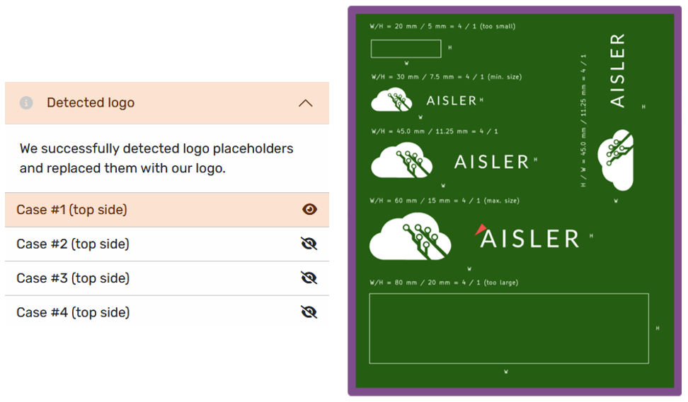
To make this easier, we provide a simple placeholder method: just draw a rectangle, and our system will automatically replace it with our logo.
How to Place the Logo
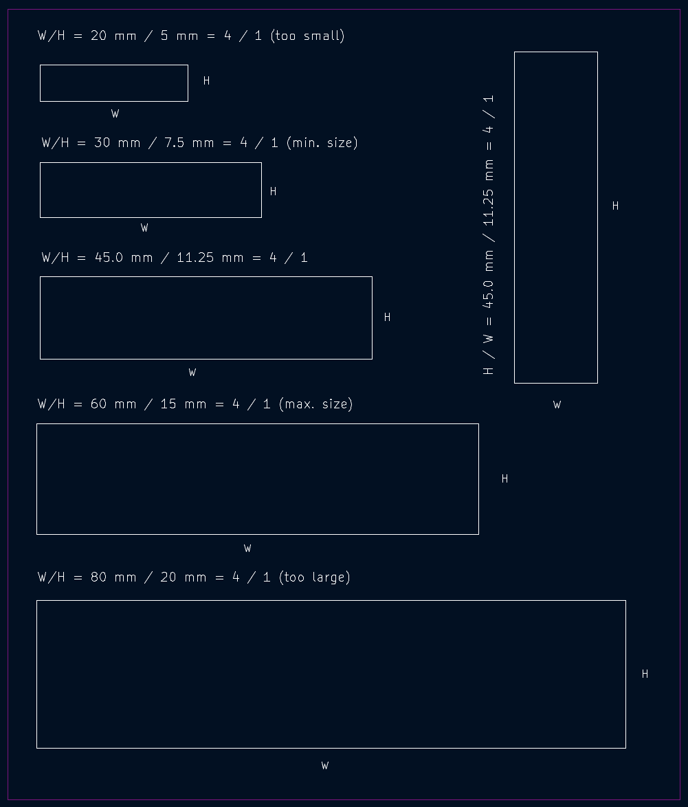
Draw a rectangle placeholder on the desired silkscreen layer and make sure the rectangle follows these rules:
- Composed of four individual lines (avoid using a rectangle tool if it causes recognition issues).
- Line width: 3.3 mil (0.08382 mm).
- Orientation: horizontal or vertical.
- Aspect ratio: 4:1 (long side / short side).
- Long side length: 30–60 mm.
Once detected, our system automatically replaces the placeholder with our logo and shows a Processing Note in our board viewer.
Why This Is Easier
- No need to import external graphics into your EDA tool.
- No risk of scaling errors or wrong layers.
- Works consistently across different CAD tools.
- Place as many placeholders as you want — each will be replaced with the logo.
Tips & Tricks
- If your EDA tool’s rectangle function prevents detection, draw the lines manually.
- Using this method will give you a discount during the checkout: