How to correct this complex PCB outline with cutouts

Hi all,

this is my first post here, nice web site / tooling btw! hope it’ll eat my screenshots (down below) which I need to even ask my question on which I am looking for help;)

I’ve got a problem with defining correct PCB outlines with cutouts using KiCad 7.

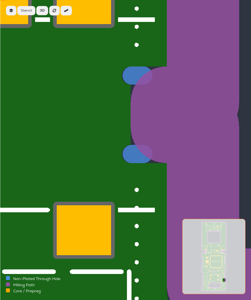
I’ve checked my PCB in an early stage using the Aisler online tools, and one issue I identified is that the outline manufacturing apparently uses both mill and drill (which is good/correct I guess?) - but still leaves small pieces of the PCB that should be gone:

The part is an audio jack, CUI Devices, SJ2-35954D-SMT-TR

The footprint of the part is the “official” one.

The Aisler PCB online check hasn’t anything to complain about (in this part), but I’m afraid the part wouldn’t fit.

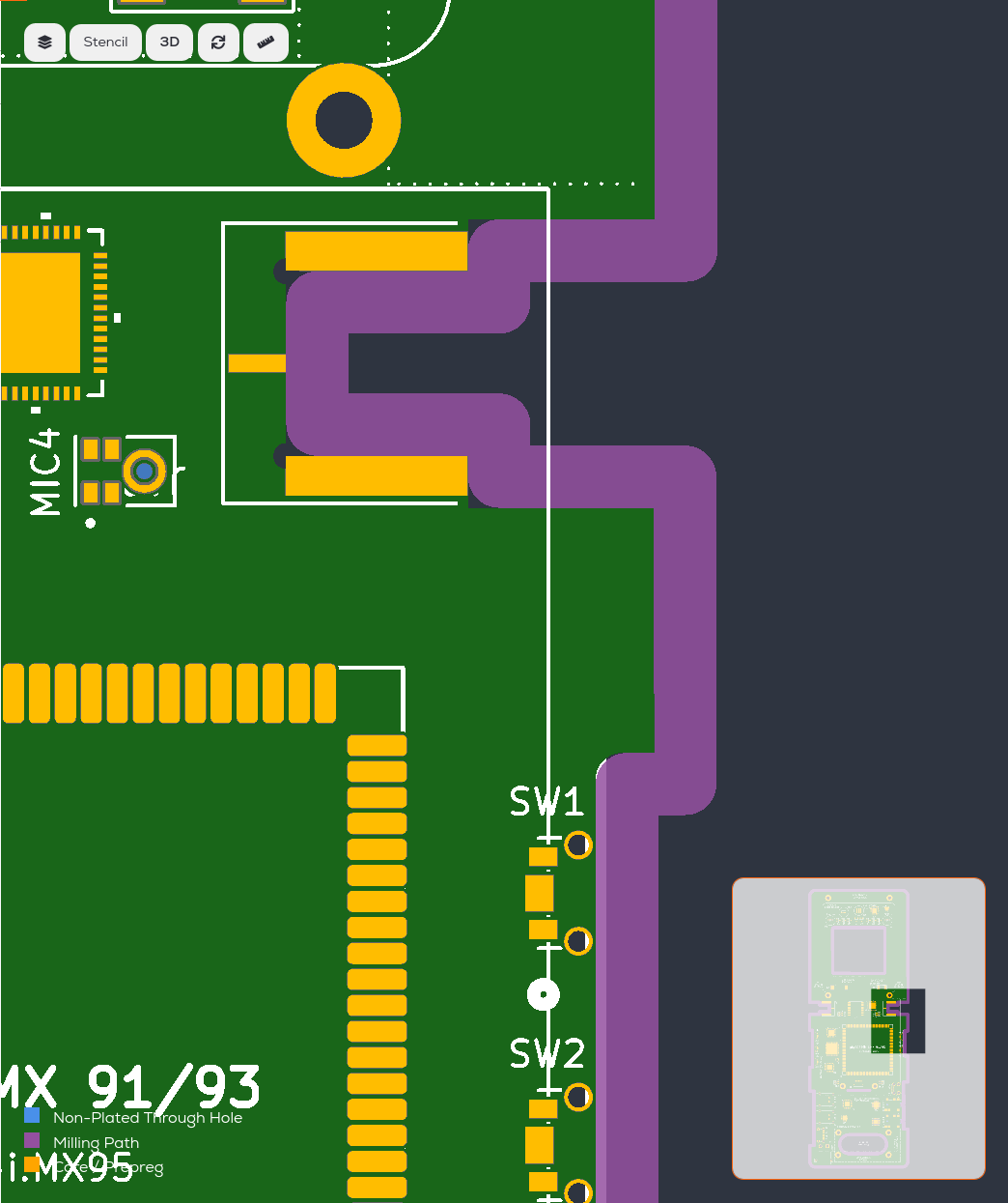
Two more problems also related to cutouts can be seen in this screenshot from the Aisler online PCB check:

The top part contains a SMA jack:

Rosenberger, 32K242-40ML5

for which I could not find a footprint, so I’ve created one based on the datasheet, but obviously it has issues (the cutout) which would also prevent the part to fit.

Finally, the bottom part shows a tiny gap in the corner next to “SW1”, the mill diameter seems slightly larger than what I used when drawing the outline in KiCad. This wouldn’t be a blocker issue … I am just wondering why?

I am sorry if those are newbie questions, I am actually a SW developer only getting into PCBs and such, so please excuse, but any tip would be absolutely appreciated.

My own footprint has bugs … I can do more experiments/design to try figuring it out … but my first issue with the CUI audio jack, I am pretty lost on this, because it is the official footprint which I use, and the 3D rendering (including Step models of the part) look perfect - but not the Aisler 3D view.

Thanks a lot,
Cheers,

/Tobias

fwiw, I’ve found sth in the posts:

  1. it seems Aisler is using a 1.8mm mill bit for all designs, including “complex” rated ones (which mine is, because it has 4 layers)

so my minor issue with the small space in the “SW1” board corner: this should be fixed to use a 1.8mm arc?

  1. rgd my SMA connector issue … apparently, @holzi has created a footprint for the exact part I am using=) coincidence.

awesome!! I will dig into that. not sure if the Aisler mill dia change breaks that or if it still works though.


but even if so, my audio jack problem remains … the part vendor’s (CUI) footprint doesn’t work … I think … not sure, as said, I’m a newbie;)

Hello,
the current version of my footprint on GitHub will not be fabricated as expected due to the change of the outline milling Tool diameter by Aisler.

The necessary changes are, however minor. I have created an update already. A fabricated board with the updated version looks just fine.

I hope that I find the time to publish the Update in the next days.

For KiCAD 7 there is now a set of Design Rule exceptions for the footprint to have a Clean DRC

Regars
Tobias

1 Like

Thank you so much for the explanation! and for publishing a new footprint which works on current Aisler setting. awesome! guess you’ll have noticed, in the meantime, I’ve taken your test board from github and replaced the generic? 3d model of the part with the one (only now?) published by Rosenberger. filed a PR to your GH repo.

However, I’m really a newbie, struggled with wrapping it up so KiCad finds all and the right things (symbol/footprint/3d) etc …

Anyways, thanks again!

Hello,
I made an update to the Footprint in Guithub. Hello,
Unfortunately, AISLER has discontinued the 6Layer stack up after just two yeas. Therefore, this project is no longer useable.

Regards,
Tobias

Hi Tobias,

yeah, I’m aware of the deprecation:( Thanks for the update in any case!

I still think an open-source footprint for a professional SMA connector that works with KiCad and Aisler and includes a professional openEMS model + measurements is worth gold!

So please continue your (OSS) work, I am following, also I’ve learned a lot just by reading your code! I am now talking more about all the openEMS stuff. Obviously what you do is much more advanced from frequ. range than I need, but still.

From my current perspective, things have moved / changed a lot in the last weeks.

I don’t want to spam the forum here with OT noise, but my goals changed, I’ve rescoped the device from “handheld” into “portable femtocell” or only “active antenna” on a separate board, and am now working with the AislerHD2L stack (also because cost), have models of 50 ohm transmission lines etc on that (even though Aisler only has documentation for AislerHD4L), and some first working planar antennas designed to 50 ohm straight including openEMS models.

Anyways. I underestimated the efforts for a newbie like me to get into EM, but I now see some light;) Currently working on getting my phased LPDA model to fly …

Cheers,
/Tobias

1 Like

Thank you for your continued interest. We didn’t provide examples for 2 L, as they are typically unsuitable for digital transmission lines due to the large distance between the signal and reference plane, resulting in large track widths.

1 Like

yes, true, it gets wider. I have only been working on lowish GHz RF in this context, and I am new to almost all of this hardware stuff. I am actually a software developer;)

fwiw, I’ve computed the trace width for the AISLER “Beautiful Boards HD 2L” PCB stack using a generic microstrip impedance calculator, the result is:

2.9mm

this is ~ 10x the width Aisler recommends for the HL 4L using outer / first inner layers.

using that trace width, I could model the PCB stackup (only the copper layers and core substrate … not the ENIG)

for modeling of a simple planar dipole in openEMS

which produces expected results (in openEMS)


I have not:

  • modeled the stack’s ENIG surface finish
  • modeled a transmission line separately (the 50 ohm line is used as a dipole feed line, and the dipole has ~64 ohm at its actual center, thus the transmission line is actually doing “impedance matching” on the fly)
  • measured things on a real PCB board

for me, other things are more pressing atm … I need to transplant my LPDA generator to the proper code like above including the HD 2L stackup and get that working.

then I will order a bunch of boards … and then the big suprise will come: does a VNA measure numbers close to my simulations?

I very much hope so. But I have never done it before. will see;)

2 Likes